(THEORY)
(ANALOG)
(DIGITAL)
(SOFTWARE)
(HOME)
A homemade receiver for GPS & GLONASS satellites
Matjaz Vidmar, S53MV (ex YU3UMV, YT3MV)
4. Homemade receiver modules for GPS & GLONASS
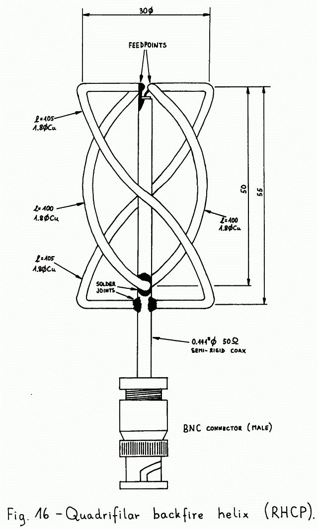
4.1. Quadrifilar backfire helix antenna
Although long-range, precision navigation systems like
GPS or GLONASS were designed to be independent as much as
possible of the performance of either transmitting or
receiving antennas, the antennas used still have some
influence on the system performance. The transmitting antennas
installed on the spacecrafts have a shaped beam to supply any
Earth-located user with the same signal strength and use the
on-board transmitter power more efficiently. Maintaining the
same signal strength is especially important in CDMA, since
the GPS C/A-codes are too short to offer a very good crosstalk
performance.
The ideal receiving antenna should have a hemispherical
radiation pattern, offering the same signal strength from
a satellite at zenith and from another satellite just above
horizon. Further, the receiving antenna should match the
transmitter polarization (RHCP) in all valid directions.
Finally, the receiving antenna should attenuate any signals
coming from undesired directions, like signals coming from
negative elevations, since these are certainly reflected
waves and the latter are a major source of measurement errors
due to their unknown propagation path.
Although a turnstile antenna (two crossed dipoles fed in
quadrature) with or without a reflector is frequently used for
satellite reception, this antenna is not very suitable for
satellite navigation for several reasons. The polarization of
a turnstile antenna is circular only in the zenith direction
and is completely linear in the horizon plane. Therefore, a
turnstile antenna offers no discrimination between the desired
RHCP direct wave and the unwanted LHCP reflected wave, since
circularly polarized waves change their sense of polarization
on each reflection. Reflected waves cause severe measurement
errors and a relatively slow and deep signal fading, so that
the receiver even looses lock on the signal.
A better alternative is a microstrip patch antenna.
A single microstrip patch resonator provides a useful
radiation pattern with a reasonably circular polarisation over
a wide range of elevations. Unfortunately the radiation
pattern of a microstrip antenna falls down to zero in the
horizon plane. Microstrip antennas are usually used when
a simple, low-profile antenna is required, usually to be
installed on a vehicle roof. Since low-elevation satellites
can not be received, a microstrip antenna usually limits the
available GDOP.
The best antenna for satellite navigation and other
applications requiring hemispherical coverage seems to be the
quadrifilar backfire helix (also called a "volute" antenna).
Such an antenna provides a shaped conical beam. The beam
shaping and cone aperture can be controlled by adjusting the
helix radius, turns pitch distance and number of turns as
described in [11]. By the way, the same type of antenna is
frequently used on low-Earth orbit satellites, like the NOAA
weather satellites.
As the GPS and GLONASS satellites already provide a
constant signal strength for Earth-located users regardless
of the satellite elevation, no particular beam shaping is
required for the receiving antenna. The optimum number of
turns of a quadrifilar backfire helix used as a GPS or GLONASS
receiving antenna seems to be between 1.5 and 3. Making a
quadrifilar backfire helix longer by increasing the number of
turns does not have much effect on the gain or the beam-cone
aperture, but it improves the beam shaping and further
attenuates the undesired lobe in the opposite direction
(downwards).
Although the best GPS receivers use such a quadrifilar
helix with 1.5 or 2 turns, such an antenna is difficult to
manufacture and test. In particular, the four helical wires
have to be fed in quadrature and there is very little space
on top of such an antenna to install the feeding network.
Further, a 2-turn backfire helix is rather large (20cm high)
for a portable receiver. If its improved pattern performance
is to be fully exploited, the direction of its axis should
not deviate too much from vertical and this is not a very
practical requirement for a portable receiver.
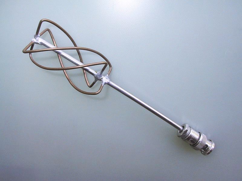
Most GPS/GLONASS receivers therefore use a simpler
antenna, usually a short one-half turn backfire helix like
shown on Fig. 16. Making the quadrifilar helix shorter
resonance effects can be used to feed the four helical
wires with the proper signal phases. In particular, one pair
of wires is made shorter to make its impedance capacitive
at the operating frequency and the other pair of wires is made
longer to make its impedance inductive at the operating
frequency.
To obtain RHCP a conventional end-fire helix has to be
wound like a right-hand screw. The backfire helix is just
opposite: to obtain RHCP the backfire helix has to be wound
as a left-hand screw, besides the proper phasing of the four
helical wires, of course! Further, the backfire helix
requires no reflector. The four helical wires are fed at one
end of the helix and shorted together at the other end of the
helix. Since the main (desired) radiation lobe is directed
towards the feedpiont and away from the shorted end, such an
antenna is called a backfire antenna.
The feedpoint impedance is in the 50ohm range,
symmetrical. A good match to 50ohms is usually sacrified for
the radiation pattern which is much more important.
Usually one of the four helical wires is replaced by a
semi-rigid coaxial cable of the same outer diameter to form
an "infinite balun". On the other hand, the performance of the
antenna is not degraded much if no balun is used like shown
on Fig. 16.
In the practical construction of a half-turn quadrifilar
helix it is especially important to respect the exact lengths
of the helical wires, since the antenna uses resonance effects
and is rather narrowband. The dimensions shown on Fig. 16 are
for the GPS L1 frequency (1575.42MHz). A GLONASS L1 antenna
should be approximately 3% smaller. Finally, an antenna for
both GPS and GLONASS L1 channels can be built by designing it
for the average of the two frequency bands.
4.2. Low-noise amplifier
In all satellite microwave receivers it is usual to
install a low-noise amplifier close to the antenna to avoid
any feedline losses and make use of the very low sky noise
temperature in the microwave frequency bands. A GPS or GLONASS
navigation receiver does not require a particularly low-noise
antenna amplifier since the omnidirectional antenna collects
lots of ground noise (300K) and the systems themselves were
designed with large margins allowing a receiver noise figure of
5dB or even more. Using a better antenna amplifier can only
bring marginal improvements.
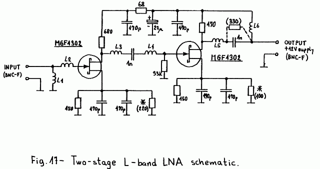
A two-stage GaAs FET antenna amplifier [12] was initially developed for a GPS receiver. This amplifier is using lumped components (coils) for input, interstage and output matching (see the circuit diagram on Fig. 17) and is constructed in free air to minimize any matching circuit losses (see the layout on Fig. 18). Further, this amplifier circuit design provides stable operation even with highly resonant sources like the described quadrifilar helix antenna and in practice the circuit resulted easily reproducible.
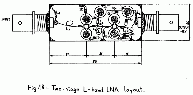
The antenna amplifier is built inside a small metal
case with the dimensions of 50mm(length)X20mm(width)X
X15mm(height) with BNC connectors for both input and output.
Since the supply voltage of +12V is fed through the output
connector, care must be exercised not to swap the two
connectors in practical use! On the other hand, the suggested
preamplifier case is small enough to avoid resonance problems
with ordinary GaAs FETs, like the MGF1302. However, if higher
gain devices or HEMTS like CFY65 are used in this amplifier
design, a small piece of absorber foam is usually required to
avoid oscillations at very high frequencies. To avoid any
additional losses at 1.5GHz, the absorber should be placed
just under the cover and only above the second stage.
The described preamplifier is a wideband device and does
not require any particular tuning. The only adjustments
necessary are the source resistors of both GaAsFETs to obtain
a suitable DC bias for both stages.
The gain of the described antenna amplifier is, depending
on the devices used, somewhere between 25dB and 35dB. This is
enough to compensate for the losses in up to 10m of RG-214
cable and the much higher noise figure of the downconverter.
Since GPS or GLONASS receivers are usually used as portable
equipment, the antenna and preamplifier are installed directly
on the top of the receiver.
4.3. GPS RF module
The GPS receiver only requires a single-frequency
(1575.42MHz) downconverter and its design is relatively
straightforward. The GPS downconverter includes two modules:
a RF module built in microstrip technology and an IF strip
built on a simple, single-sided printed circuit board.
The circuit diagram of the GPS RF module is shown on
Fig. 19. The GPS RF module includes three RF amplifier stages
and the first downconversion mixer. The amplifier stages are
identical and use silicon MRF571 transistors. Much of the gain
provided by these transistors is lost in the microstrip
filters, since the latter are etched on a lossy but inexpensive
glassfiber-epoxy laminate.
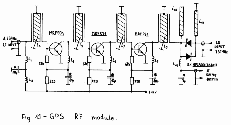
The first downconversion to 102MHz is performed by a
harmonic mixer using two anti-parallel Schottky diodes HP2900,
BA481 or similar. Such a mixer has a higher noise figure than
conventional diode mixers, especially when using the suggested
low frequency diodes. On the other hand, the required local
oscillator signal is at 736MHz, only half of the frequency
required for the downconversion (1473MHz).
The RF module circuit includes a network to supply with
+12V the GaAs FET preamplifier through the RF cable. On the
other hand, the +12V supply voltage for the RF module itself
is taken out of the IF converter, after being filtered by a
choke and a 100uF capacitor.
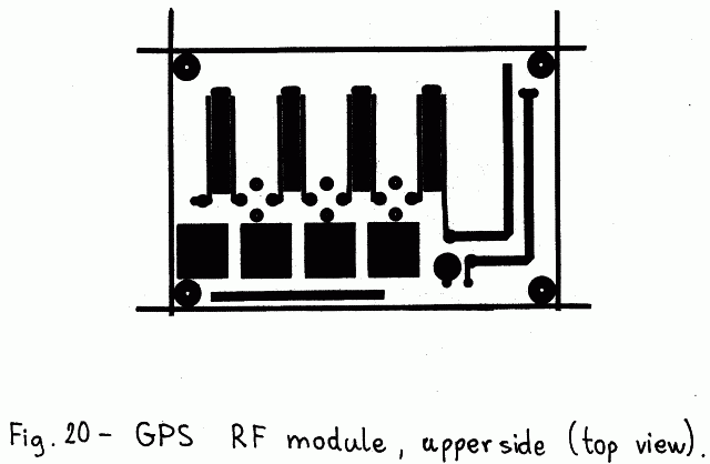
The RF module is built in microstrip technology on a double-sided board made of 0.79mm thick glassfiber-epoxy. The upper side is shown on Fig. 20 while the lower side is not etched. The location of the components is shown on Fig. 21. Before installing the components, L3, L5, L7, L9 and L12 should be grounded by soldering small U-shaped pieces of wire at the marked locations.
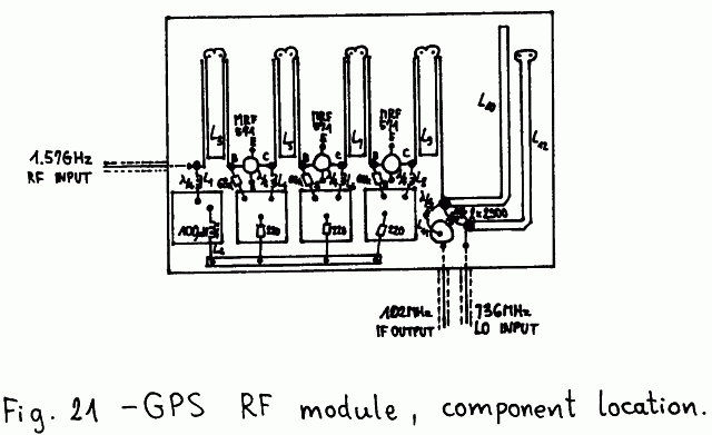
L1, L4, L6, L8 and L11 are quarter-wavelength chokes.
These are made from about 6cm of 0.15mm thick copper
enamelled wire, tinned for about 5mm at each end. The remaining
wire is wound on a 1mm inner diameter and the finished chokes
are small self-supporting coils. On the other hand, L2 is a
commercial 100uH "molded" choke.
It is recommended to use thin teflon coax like RG-188 for
the internal RF wiring of the GPS receiver. The braid of the
cable should be soldered directly to the microstrip groundplane
while the central conductor reaches the upper tracks through
a hole in the printed-circuit board. To avoid shorts, the
copper plating around this hole on the groundplane side should
be carefully removed using a much larger (3mm) drill tip.
The GPS RF module needs some adjustments of the striplines
and these are best performed after all of the receiver hardware
is assembled. L3, L5, L7 and L9 usually need to be trimmed
shorter by about 1mm at the open end to achieve the maximum
gain at 1575MHz. On the other hand, L10 and L12 may need some
small pieces of copper foil (about 7mmx7mm) at different
locations along these striplines to achieve the best noise
figure from the diodes actually used in the mixer.
4.4. GPS IF converter
The GPS IF strip includes a second downconversion to
10MHz, signal amplification and limiting at 10MHz and the
generation of all required local oscillator and clock signals
from a single master frequency reference.
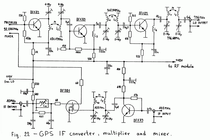
The second downconversion to 10MHz and the LO frequency generation is included in the GPS IF converter module shown on Fig. 22 and Fig. 23. The GPS IF converter module includes a 6139kHz crystal oscillator (Fig. 23). This frequency is used both for signal sampling and suitably multiplied for both downconversions. Since the required short term stability is very high, in the 1.E-9 range, to be able to demodulate the 50bps PSK navigation data, the crystal oscillator has its own supply regulator 7805 and is followed by two buffer stages.
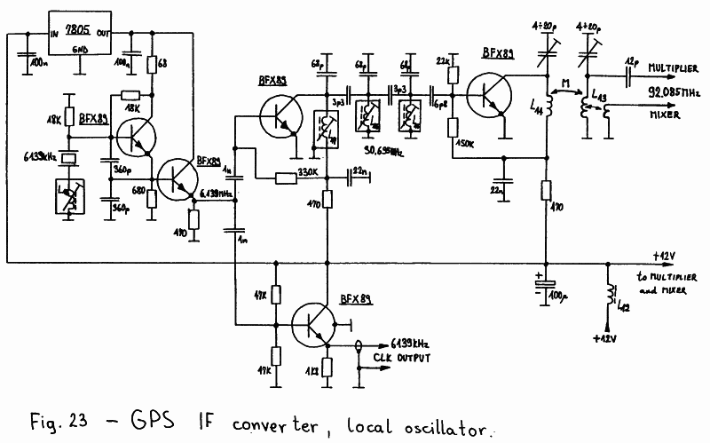
The crystal oscillator output frequency is first
multiplied by five to obtain 30.7MHz and then by three to
obtain the 92MHz required for the second downconversion. Three
additional frequency-doubler stages are required to obtain the
first downconversion signal at 736MHz from the available 92MHz
signal. The design of all multiplier stages is similar and is
using two tuned circuits in each stage except for the first
stage, where three tuned circuits are necessary due to the
higher multiplication factor.
The 102MHz IF signal is first amplified (BFX89) and then
filtered (L9 and L10). The second mixer is a simple dual-gate
MOSFET mixer (BF981). The selectivity provided by the tuned
circuits at 102MHz (L9 and L10) and at 10MHz (L11) is already
comparable to the GPS C/A-code signal bandwidth (2MHz).
In fact, L11 already requires damping resistors to achieve the
required bandwidth.
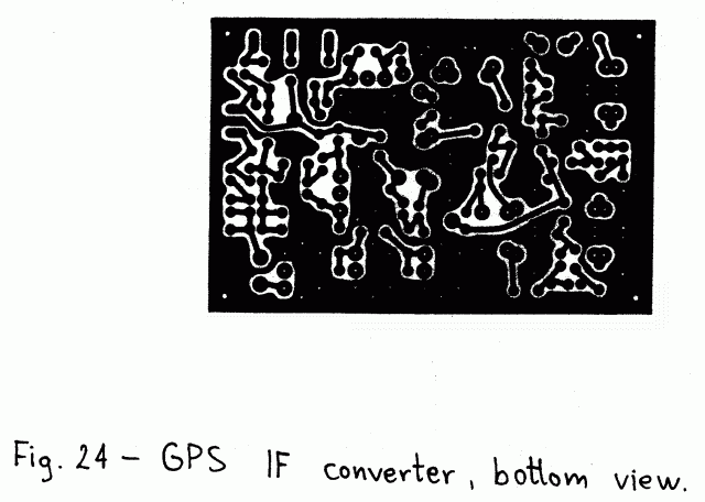
The GPS IF converter is built on a single-sided board as shown on Fig. 24. The location of the components is shown on Fig. 25. Due to the limited space all of the resistors are installed vertically. The capacitors are conventional ceramic discs (except for 100uF) with a pin spacing of 5mm. Capacitive trimmers are plastic foil types of 7.5mm diameter: green 4-20pF and yellow 2-10pF. There is also a wire jumper marked with "A".
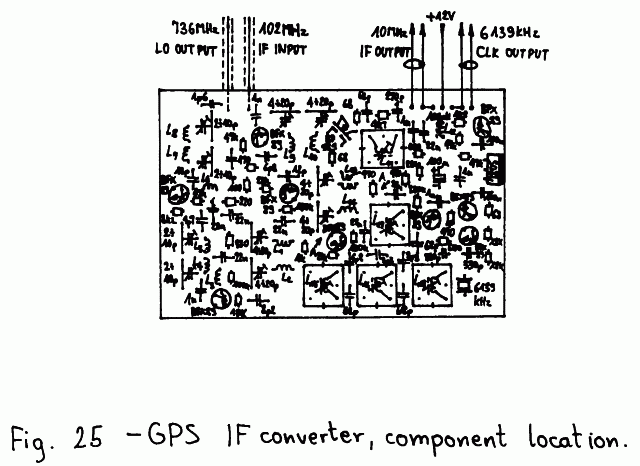
The BFX89 is used as an universal RF transistor in this
module and has many possible replacements: BFY90, BFW30 etc.
The four leads of the BF981 MOSFET are bent so that the device
is inserted in the printed-circuit board with the marking
towards the board. The 7805 regulator does not require a
heat sink provided that it is a TO-220 version.
The GPS IF converter includes several inductors. Most of
them are air-wound, self-supporting coils wound with copper
enamelled wire of either 0.5mm or 1mm diameter. The turns of
these coils are not spaced and the leads go straight through
the printed-circuit board without any additional bending or
forming. In these way the coils themselves have about 1/4 of
a turn less than specified in the following paragraph.
L1 and L2 have 3 turns each of 1mm wire wound on a 4mm
inner diameter. L3 has 5 turns of 0.5mm wire wound on a 3mm
inner diameter. L4 and L5 have two turns each of 1mm wire
wound on a 3mm inner diameter. L6 has 3 turns of 0.5mm wire
wound on 3mm inner diameter. L7 and L8 have one single turn
(or "U" loop) of 1mm wire with a 3mm inner diameter.
L9 and L10 have 5 turns each of 0.5mm wire on a 4mm inner
diameter. Finally, L13 and L14 have 6 turns each of 0.5mm
wire wound on a 4mm inner diameter. L13 has an additional
coupling loop of one single turn around the main winding.
L11, L15, L16, L17 and L18 are wound on standard cores
for IF transformers (Toko or Mitsumi) with the external
dimensions of 10mmX10mm. L11 should have about 4.5uH and in
practice this means 15 turns of 0.15mm diameter copper
enamelled wire on a 10.7MHz IF transformer core set including
a fixed central ferrite core, an adjustable ferrite cup,
various plastic support parts and a metal shielding can.
L15, L16 and L17 should have about 0.4uH and in practice
have 6 turns of 0.15mm diameter copper enamelled wire on a
36MHz IF transformer core set including a plastic support
with a central adjustable ferrite screw, a plastic cap and
a metal shielding can.
The exact value of L18 depends on the crystal used and
the frequency required. In all of the prototypes built
inexpensive computer crystals designed for 6144kHz were used.
These require quite a large inductance to be pulled 5kHz
down to about 6139kHz. An inductance around 40uH is required
for this shift. The exact value depends much on the crystal
used and the parasitic capacitances of the circuit. Since the
performance of the GPS receiver depends on the stability of
this master crystal oscillator, also L18 needs to be very
stable. Therefore a 36MHz IF transformer core set is
recommended and the latter requires about 60 turns of 0.08mm
diameter copper enamelled wire.
Finally, L12 is a 100uH "molded" choke.
The GPS IF converter has several connections. The two coax
cables carrying IF and LO signals to the RF module and the
+12V supply wire for the RF module are all soldered directly
to the bottom side of the IF converter module. The 10MHz IF
output, the 6139kHz clock output and the +12V supply
voltage are available on a 7-pin connector obtained from a
piece of a good-quality IC socket with round contacts.
The GPS IF module requires several adjustments, but the
crystal oscillator should be adjusted first to roughly 6139kHz.
Then the multiplier chain should be adjusted. Each multiplier
stage should be adjusted to provide the maximum signal at the
required frequency to the next stage. The levels of the RF
signals can be easily monitored with a DC voltmeter, since
they are rectified by the BE junction of the next stage.
Without any RF input, the DC voltage is set to about 0.7V
across the BE junction. When the multiplier chain is operating
correctly, this voltage should decrease down to about zero
and may even become negative. If the transistor base goes
more negative than -0.5V, RF transistors may be damaged and
this should be avoided by decreasing the values of the coupling
capacitors.
Of course, the voltmeter required for these adjustments
should only be connected through a RF choke to avoid disturbing
the RF circuit. A 10kohm resistor may also be used as a RF
choke. In this way all of the multiplier stages can be adjusted
except the last one to 736MHz, since no BE junction follows
this stage. The level of the 736MHz signal is monitored in a
different way, by connecting a DC ohmmeter to the IF output of
the mixer. The higher the LO signal level, the lower the
resistance measured by the ohmmeter.
The signal circuits (L9, L10 and L11) are best adjusted
after the receiver is completely assembled, since the following
IF amplifier has a S-meter output. A grid-dip meter can be
used as a signal source at 102MHz. The trimmers in parallel to
L9 and L10 tune almost to their maximum capacity and L10 may
sometimes require an additional capacitor in parallel.
The final adjustment of the signal circuits is best performed
on a real GPS signal obtained from a directional antenna
(a 15 turn helix or a small dish) pointed to a GPS satellite.
Finally, the crystal oscillator should be adjusted to the
exact frequency required by the software. For the current
version V122 the exact frequency is 6139.050kHz, but this may
change in the future. The exact frequency is specified in
the program listing.
4.5. GLONASS RF module
The GLONASS receiver requires a tunable downconverter
across all of the 25 GLONASS channels spacing from 1602MHz to
1615.5MHz, therefore its design is more complicated than the
GPS counterpart. The GLONASS downconverter is divided into
four modules for shielding purposes and differences in the
construction technology: a RF module and a PLL synthesizer
converter built in microstrip technology and an IF converter
and synthesizer logic built on simple, single-sided printed
circuit boards.
The circuit diagram of the GLONASS RF module is shown
on Fig. 26. The GLONASS RF module includes two selective RF
amplifier stages, the first receiver mixer to the first
(fixed) IF of 118.7MHz, and a VCO followed by a buffer stage.
The two RF amplifier stages are identical and use MRF571
transistors. Since the GLONASS RF module is built on a lossy,
but thicker laminate than GPS, the losses in the RF filters
are lower and two amplifier stages provide enough gain.
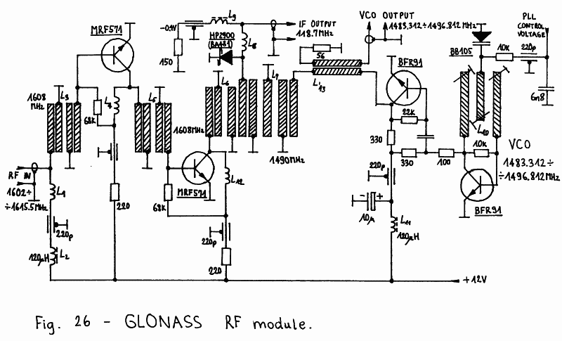
The VCO includes an amplifier (BFR91) and a
highly-selective interdigital filter feedback network. Such
a VCO can only cover a very limited frequency range (about 10%
around the central frequency), but its phase noise is very
low. The VCO is tuned by a BB105 varicap in the central finger
of the interdigital feedback network.
The VCO is followed by a buffer stage with another BFR91.
A microstrip coupler takes part of the VCO output signal to
drive the PLL circuits. The VCO and RF signals are then
combined in an interdigital filter network to feed the
mixer diode HP2900 or BA481.
The GLONASS RF module circuit includes a network to supply
with +12V the GaAs FET preamplifier through the RF cable.
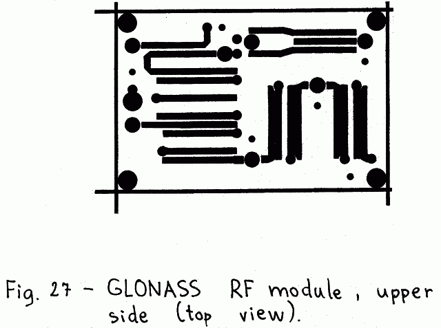
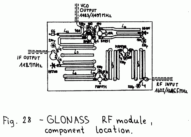
The GLONASS RF module is built in microstrip technology on a double-sided board made of 1.57mm thick glassfiber-epoxy. The upper side is shown on Fig. 27 while the lower side is not etched. The location of the components is shown on Fig. 28. Before installing the components, the resonators of L3, L5, L6 and L7 should be grounded by soldering short pieces of 1mm diameter copper wire at the marked locations. The transistors and diodes are installed in 6mm diameter holes in the printed circuit board.
L1, L4, L8 and L12 are quarter-wavelength chokes. These
are made from about 6cm of 0.15mm thick copper enamelled wire,
tinned for about 5mm at each end. The remaining wire is wound
on a 1mm inner diameter and the finished chokes are small
self-supporting coils. On the other hand, L2, L9 and L11 are
commercial 120uH "molded" chokes.
RF interconnections inside the GLONASS receiver are made
with thin teflon coax like RG-188, installed just like in the
GPS receiver front end. On the other hand, GLONASS microstrip
modules include feedthrough capacitors to save space on the
printed-circuit boards. The feedthrough capacitors are
soldered to the microstrip groundplane from the bottom side.
Some components, like chokes and resistors in the supply
network, are also installed on the bottom side of the
microstrip boards.
The GLONASS RF module only needs few adjustments, mainly
to the VCO feedback network. To cover the desired frequency
range, the central finger usually needs to be trimmed shorter
by several mm. The two side fingers may need adjustments if
the VCO stops oscillating at band edges. The remaining
interdigital filters usually do not need any adjustments to
provide the best performance in the desired frequency range.
If the VCO is operating correctly, the mixer diode will
provide a rectified voltage of about -0.4V across the 150ohm
resistor.
4.6. GLONASS IF converter
The GLONASS IF strip includes a second downconversion to
10.7MHz, signal amplification and limiting at 10.7MHz and the
generation of the required local oscillator and clock signals
from a single master frequency reference.
The second downconversion to 10.7MHz and the LO frequency
generation is included in the GLONASS IF converter module shown
on Fig. 29. The GLONASS IF converter module includes a 18MHz
master crystal oscillator. This frequency is used, divided by
four, for signal sampling, divided by 32 as the PLL reference
frequency and suitably multiplied for the second signal
downconversion and for the PLL downconversion.
The GLONASS IF module only includes the oscillator and
some multiplier stages. The dividers are located in the PLL
synthesizer logic module and the last frequency multiplier is
in the PLL synthesizer converter. Like in the GPS receiver,
the required short term stability is very high, in the 1.E-9
range, to be able to demodulate the 50bps PSK navigation data
Therefore the crystal oscillator has its own supply regulator
7805 and is followed by two buffer stages just like in the
GPS IF converter module.
The crystal oscillator output frequency is first
multiplied by three to obtain 54MHz. This signal is then
doubled to 108MHz for the second downconversion and multiplied
by three to obtain 162MHz to drive the PLL synthesizer
converter, using two separate multiplier stages fed by the
same 54MHz signal. The 162MHz signal is further amplified in
a buffer stage (BFR96) to drive the SRD multiplier in the
PLL synthesizer converter.
Since the described GLONASS receiver includes a more
complicated RF front-end than GPS, more filtering is required
in all multiplier stages to avoid spurious frequencies.
Therefore multiplier stages may have three or even more tuned
circuits on their outputs.
The 118.7MHz IF signal is filtered (L9, L10 and L11) and
amplified (BFX89). The second mixer is a simple dual-gate
MOSFET mixer (BF981). The selectivity provided by the tuned
circuits at 118.7MHz (L9, L10 and L11) and at 10.7MHz (L12) is
already comparable to the GLONASS C/A-code signal bandwidth
(1.2MHz). In fact, L12 already requires damping resistors to
achieve the required bandwidth.
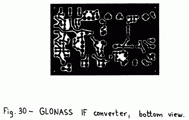
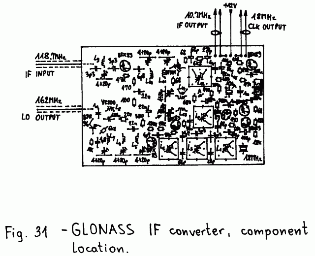
The GLONASS IF converter is built on a single-sided board as shown on Fig. 30. The location of the components is shown on Fig. 31. Due to the limited space all of the resistors are installed vertically. The capacitors are conventional ceramic discs (except for 100uF) with a pin spacing of 5mm. Capacitive trimmers 4-20pF are a plastic foil type of 7.5mm diameter, marked with a green body. There is also a wire jumper marked with "A".
The BFX89 is used as an universal RF transistor like in
the GPS IF converter. Also the BF981 is installed just like
in the GPS IF converter module and a TO-220 case 7805 regulator
is recommended so that no heat sink is required.
The GLONASS IF converter includes several inductors. Most
of them are air-wound, self-supporting coils wound with copper
enamelled wire of 0.5mm diameter. The turns of these coils are
not spaced and the leads go straight through the
printed-circuit board without any additional bending or
forming. In these way the coils themselves have about 1/4 of
a turn less than specified in the following paragraph.
L5, L6 and L7 have 4 turns each wound on a 3mm inner
diameter. L9, L10 and L11 have 4 turns wound on a 4mm inner
diameter. L13 and L14 have 5 turns wound on a 4mm inner
diameter. L14 has an additional coupling loop of one single
turn around the main winding.
L1, L2, L3, L4 and L12 are wound on standard cores
for IF transformers (Toko or Mitsumi) with the external
dimensions of 10mmX10mm. L12 should have about 4.5uH and in
practice this means 15 turns of 0.15mm diameter copper
enamelled wire on a 10.7MHz IF transformer core set including
a fixed central ferrite core, an adjustable ferrite cup,
various plastic support parts and a metal shielding can.
L2, L3 and L4 should have about 0.13uH and in practice
have 3 turns of 0.3mm diameter copper enamelled wire on a
36MHz IF transformer core set including a plastic support
with a central adjustable ferrite screw, a plastic cap and
a metal shielding can.
The exact value of L1 depends on the crystal used and
the frequency required. In all of the prototypes built
inexpensive computer crystals designed for 18000kHz, series
resonance, were used. These require a small inductance
in series to compensate for the feedback capacitors of the
oscillator network. In practice about 2uH were required,
corresponding to 16 turns of 0.15mm diameter copper enamelled
wire on a 36MHz IF transformer core set.
Finally, L8 is a VK200 "six-hole" ferrite choke and L15
is a 100uH "molded" choke.
The GLONASS IF converter module has several connections.
The two cables carrying the 118.7MHz IF from the RF module and
the 162MHz LO to the PLL synthesizer converter are all soldered
directly to the bottom side of the IF converter module.
The 10.7MHz IF output, the 18MHz clock output and the +12V
supply voltage are available on a 7-pin connector obtained from
a piece of a good-quality IC socket with round contacts.
In the GLONASS IF converter module the multiplier stages
should be aligned first, just like in the similar GPS module.
However, only the output of the first multiplier stage to 54MHz
can be monitored as a dip of the following stage base voltage.
The output of the 108MHz multiplier may be observed as a dip
in the drain voltage of the BF981 mixer, while the output of
the 162MHz multiplier may be measured as the rectified voltage
by the SRD multiplier in the PLL synthesizer converter.
The signal circuits (L9, L10, L11 and L12) are best
adjusted after the receiver is completely assembled, since the
following IF amplifier has a S-meter output. A grid-dip meter
can used as a signal source at 118.7MHz. The trimmers in
parallel to L9, L10 and L11 tune almost to their maximum
capacity. The final adjustment of the signal circuits is best
performed on a real GLONASS signal obtained from a directional
antenna (a 15 turn helix or a small dish) pointed to a GLONASS
satellite.
Finally, the crystal oscillator should be adjusted to the
exact frequency required by the software. For the current
version V39 the exact frequency is 18000.000kHz, but this may
change in the future. The exact frequency is specified in
the program listing.
4.7. GLONASS PLL synthesizer converter
A single-channel GLONASS receiver requires a fast-settling
frequency synthesizer, since the receiver is continuously
switching among different frequency channels. Besides this
requirement the synthesizer should have a low phase noise.
To limit group-delay variations the synthesizer should supply
a variable frequency already to the first downconverter.
All these requirements ask for a PLL synthesizer with
a frequency downconverter in the feedback loop, to decrease
the divider modulo and increase the loop gain. Therefore, the
GLONASS PLL synthesizer includes a VCO in the RF module,
a downconverter and conventional PLL synthesizer logic like
variable modulo dividers and a frequency/phase comparator.
The circuit diagram of the GLONASS PLL synthesizer
converter is shown on Fig. 32. The circuit includes another
buffer stage for the VCO signal around 1490MHz, a step-recovery
diode (SRD) frequency multiplier by 9, to get 1458MHz from
the available 162MHz, a mixer diode and an IF amplifier stage.
The VCO buffer stage (BFR90) is required to avoid getting any
unwanted spurious signals back in the GLONASS RF module.
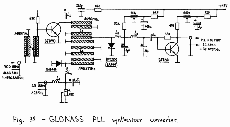
The SRD multiplier uses a very inefficient silicon
PN-junction diode 1N4148. Other diodes like VHF TV tuner
bandswitching diodes (BA182 or BA482) provide an up to 20dB
stronger signal at 1458MHz in the same circuit, but a higher
signal level is not required here and it is even harmful,
since it may get in the RF module and cause unwanted mixing
products. In practice it is thus convenient to keep the
1458MHz signal level low and drive the mixer diode into
the nonlinear region with the 1490MHz VCO signal.
To avoid any spurious generation all signal levels are
kept low. Even the buffered VCO signal amounts to only a few
hundred mV on the mixer diode HP2900 (or BA481) while the
1458MHz signal level is much lower. To operate efficiently at
low signal levels the mixer diode receives a DC bias current.
The PLL IF signal then needs much amplification to reach
the TTL level required by the variable-modulo counter. The
first PLL IF amplifier stage (BFR90) is built in the PLL
converter module. The following PLL IF amplifier stages are
located in the PLL synthesizer logic module for shielding
purposes, since harmonics of the PLL IF fall in the first IF
(118.7MHz) frequency range of the described GLONASS receiver.
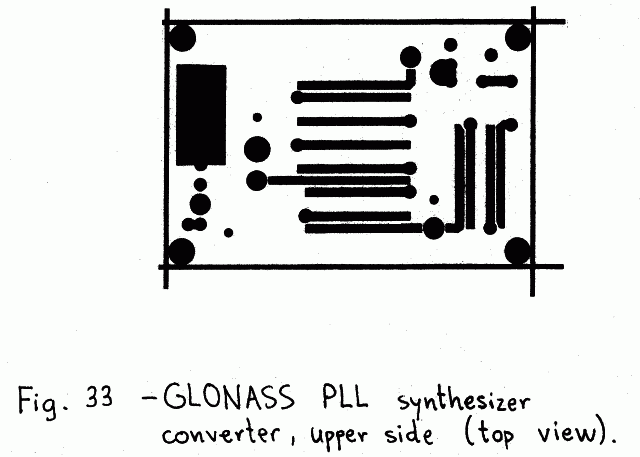
The GLONASS PLL synthesizer converter is built in microstrip technology on a double-sided board made of 1.57mm thick glassfiber-epoxy. The upper side is shown on Fig. 33 while the lower side is not etched. The location of the components is shown on Fig. 34. Before installing the components, the resonators of L1, L3 and L4 should be grounded by soldering short pieces of 1mm diameter copper wire at the marked locations. The transistors and diodes are installed in 6mm diameter holes in the printed circuit board.
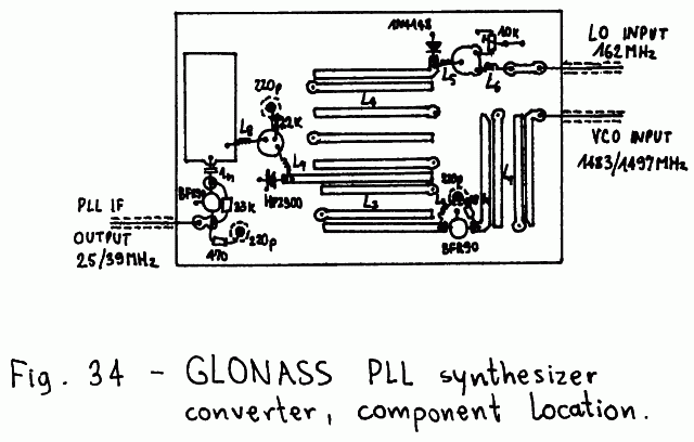
L2, L5, L7 and L8 are quarter-wavelength chokes. These
are made from about 6cm of 0.15mm thick copper enamelled wire,
tinned for about 5mm at each end. The remaining wire is wound
on a 1mm inner diameter and the finished chokes are small
self-supporting coils. L6 is a self-supporting coil with 3
turns of 0.5mm diameter copper enamelled wire wound on a
3mm inner diameter.
The microstrip filters in the GLONASS PLL synthesizer
converter usually do not require any trimming. The 10kohm
trimmer for the SRD bias current is usually set to 5kohm.
The SRD multiplier will operate correctly if the rectified
DC voltage by the 1N4148 diode amounts to about 2V.
4.8. GLONASS PLL synthesizer logic
To convert the frequency range form 1602MHz to 1615.5MHz
down to 118.6875MHz, the VCO must operate in the frequency
range from 1483.3125MHz to 1496.8125MHz. Subtracting 1458MHz
in the PLL synthesizer converter, this frequency range is
downconverted to 25.3125MHz to 38.8125MHz. The latter frequency
range corresponds to integer multiples ranging between 45 and
69 of the GLONASS channel spacing of 562.5kHz.
The design of the PLL synthesizer logic is therefore
straightforward and the corresponding circuit diagram is shown
on Fig. 35. The PLL synthesizer logic includes a PLL IF
amplifier, a variable modulo divider for the PLL IF, a fixed
divider by 32 to obtain the 562.5kHz reference and a
frequency/phase comparator.
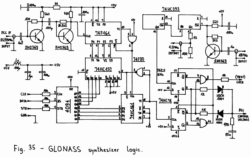
The PLL IF signal in the range from 25MHz to 39MHz is
first amplified to a TTL level in a two stage amplifier.
The gain of this amplifier is set higher than required to
have a considerable safety margin. The base bias resistor
of the second stage may need some trimming although the
suggested value of 2.2kohm will usually work.
The programmable modulo counter is built from two
synchronous counters: a 74F161 and a 74HC161. A 74Fxxx counter
is required in the first stage to operate reliably at the
highest frequency, since the PLL IF may be several tens of MHz
above 39MHz in the unlocked state!
The counter feedback network includes an inverter and a
74HC157 multiplexer. The modulo of the second counter (74HC161)
is programmed directly. The modulo of the first counter
(74F161) is set to 10 except during the last state of the
second counter, when the 74HC157 switches the 74F161 preset
inputs to the 4094 outputs. In this way setting the modulo of
the second counter changes the whole divider modulo in steps
of 10, while setting the modulo of the first counter during
the last cycle only provides the single-count steps.
The 4094 is a 8-bit shift register with output latches.
It is used as a serial-to-parallel interface driven by the
computer. Of the eight available output lines, four are used
to control the modulo of the 74HC161 counter and the other
four to control the modulo of the 74F161 during the last cycle
of the 74HC161. One should be especially careful when
programming the modulo of the divider: the data is inverted
and the first divider modulo should never be set too low to
allow for the delays in the slower 74HCxxx logic!
The 18MHz master reference frequency is also amplified to
TTL level in a single-stage amplifier (2N2369). A 74HC393
counter divides this frequency by four to obtain the 4500kHz
sampling frequency and by 32 to obtain the PLL reference
frequency. The 4500kHz signal is attenuated with a resistor
network to limit spurious radiations. It is then amplified
back to TTL level in the dedicated DSP hardware module.
The frequency/phase comparator is a charge-pump circuit
including two D-flip-flops (74HC74), a feedback network with
a NAND gate and charge-pump switches with Schottky diodes.
The backlash problem is solved by making the charge-pump
circuit faster than the feedback network. This does not
make the phase detector linear yet, but provides a stable
locking point for the PLL with no dead zone and produces a
very clean synthesizer signal spectrum. An additional NAND
gate provides a LOCK signal for test purposes.
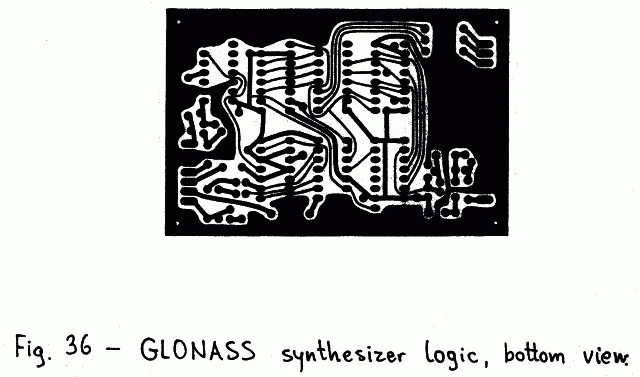
The GLONASS PLL synthesizer logic is built on a single-sided printed circuit board as shown on Fig. 36. The location of the components is shown on Fig. 37. There are three wire jumpers on this board and two of them are installed below the 74HC157 multiplexer. A complex single-sided board also places some constraints on the installation of the resistors: those with a 10mm hole spacing are installed horizontally while the others are installed vertically to save space. All of the capacitors are ceramic with a 5mm pin spacing, including the 1uF (multilayer).
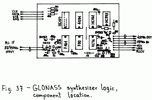
L1 is a commercial 100uH "molded" choke. The module has
three connectors with 3, 4 and 7 contacts, made from pieces
of good-quality IC sockets. The integrated circuits should
be soldered directly on the board except for the 4094. It
is recommended to install this IC on a socket so that
it can be removed from the circuit and replaced by wire
jumpers to be able to test the synthesizer without the
computer running.
The GLONASS synthesizer logic may require a single
adjustment: the bias resistor for the second PLL IF
amplifier stage. This may be adjusted if the output
DC voltage deviates much from 1.3V (with no input signal) or
if the programmable counter does not operate reliably.
4.9. GPS/GLONASS second IF amplifier
Both GPS and GLONASS receivers require a limiting IF
amplifier at the final IF frequency around 10MHz. The circuit
diagram of this amplifier is shown on Fig. 38. The GPS/GLONASS
second IF amplifier includes a first stage with a bipolar
transistor BFX89 and a second stage with the integrated
circuit CA3089.
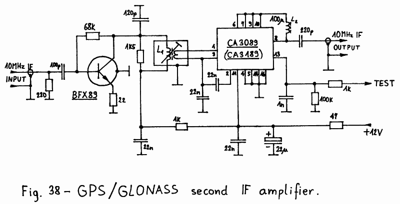
The gain of the first stage is limited by the 22ohm
resistor in the emitter circuit. The first stage is followed
by a tuned circuit (L1) to limit broadband noise and avoid
amplifying various spurious signals from the many oscillators
inside a GPS or GLONASS receiver. The damping resistor in
parallel with L1 sets the bandwidth of this tuned circuit
to be comparable to the GPS or GLONASS signal bandwidth.
The second stage uses a popular FM IF strip integrated
circuit. The latter provides wideband amplification and
limiting, while the discriminator section of this integrated
circuit is not used here. The limited IF output is available
on pin 8 and the signal level amounts to a few hundred
millivolts at 10MHz. This is not enough to drive the following
TTL logic directly and the remaining gain is built inside the
dedicated DSP hardware module.
The CA3089 integrated circuit includes a S-meter output.
The latter is of little use during actual receiver operation,
since the satellite signal levels are comparable to noise in
the wideband IF. In the case of a GPS receiver, the S-meter
output can only show the sum of all of the signals present.
On the other hand, the S-meter output is very useful during
receiver testing and alignment of the RF, first and second IF
tuned circuits.
Both GPS and GLONASS receivers include a S-meter function
inside the narrowband IF processing. Since the latter is done
in software, the real receiver S-meter as displayed on the LCD
is just another software function and is NOT related to the
hardware S-meter output of the IF strip.
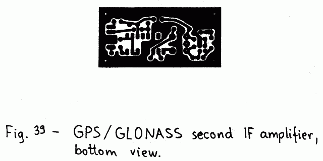
The GPS/GLONASS second IF amplifier is built on a single-sided printed circuit board as shown on Fig. 39. The location of the components is shown on Fig. 40. Due to the limited space all of the resistors are installed vertically. The capacitors are conventional ceramic discs (except for 22uF) with a pin spacing of 5mm.
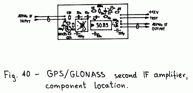
L1 is wound on a 10.7MHz IF transformer core set
including a fixed central ferrite core, an adjustable ferrite
cup, various plastic support parts and a metal shielding can.
The primary (resonant) winding of L1 has 10 turns of 0.15mm
diameter copper enamelled wire, corresponding to an
inductance of about 2uH. The secondary (link) winding has
two turns of the same wire. L2 is a 100uH "molded" choke.
The second IF amplifier module has two connectors: a
2-pin connector for the input and a 5-pin connector for the
output and supply voltage, obtained from pieces of
a good-quality IC socket with round contacts.
The tuned circuit with L1 is best adjusted after the GPS
or GLONASS receiver is completely assembled, finding the
maximum DC voltage on the "test" S-meter output in the same
IF module. The final adjustment of all signal circuits is
best performed on a real satellite signal obtained from a
directional antenna (a 15 turn helix or a small dish) pointed
to an operating navigation satellite. A directional antenna
should provide a higher-than-usual signal-to-noise ratio of
more than 10dB already in the wideband IF. A high SNR is
required to tune the circuits to the signal peak and not to
noise or some spurious signals while observing the voltage
on the "test" S-meter output.
* * * * *