1. NBP hardware
Any protocol specification is dead without practical implementations on working hardware. NBP is a quite simple protocol that requires both little memory and little processing power. Of course, the handling of all NBP variables is much easier in 32-bit registers. The choice of suitable hardware also depends on the desired bit rate.
Both the "Megabit KISS/SLIP TNC" and the "TNC for 10Mbps", described in the AX.25 section of this article, could be used in KISS mode running NBP on a host computer without any modification to their existing firmware. The latter could also be rewritten to handle the whole NBP without any support from a host computer. This should be relatively easy since NBP is much simpler than AX.25 for example.
Both above TNCs are based on a very old microprocessor MC68HC000, one of the first that had 32-bit internal registers. Both TNCs include many expensive components that require lots of work for the assembly. Worst of all, HDLC is no longer being used and hardware HDLC controllers disappeared from the market. The SAB82532 HDLC controlled used in the TNC for 10Mbps includes an excellent handling of its internal FIFO buffers, but today it is no longer available nor it does not have any valid successors.
Fortunately, new microprocessors and microcontrollers have enough computing power to implement HDLC in software up to several megabits per second. Their 32-bit microprocessor, RAM and FLASH memory and several different peripherals are now integrated on a single chip. Such a system-on-a-chip component only requires a simple, single-sided printed-circuit board to bring out signal lines to connectors and keep care of the power supply, clock and reset.
The printed-circuit board for a system-on-a-chip component can be single-sided with SMD components on one side and through-hole components as well as connectors on the other side. Two or more such boards can be stacked one over another to save space:
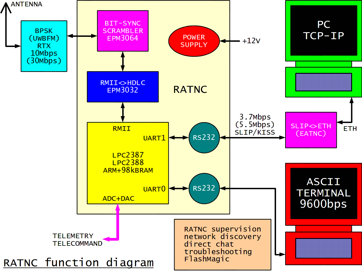
The "Advanced TNC" for NBP is currently an Arm TNC, based on 32-bit ARM microcontrollers of the LPC2xxx family manufactured by NXP (Philips). The basic ATNC supports NBP on the radio side up to 3Mbps and different KISS/SLIP protocols on the wire side up to 3.7Mbps. All software is written in ARM assembler, using 32-bit ARM instructions and optimized for maximum performance. Therefore time-critical parts are written as long linear programs to avoid FLASH and CPU pipeline losses due to program jumps in loops.
Besides the basic ATNC, the family also includes the Advanced-ATNC (AATNC), the Ethernet-ATNC (EATNC), the Modem-ATNC (MATNC), the RMII-ATNC (RATNC) and the SPI-ATNC (SATNC). The AATNC is identical to the ATNC except for the microcontroller used: the faster LPC23xx with more on-chip RAM and KISS/SLIP up to 5.5Mbps in place of the LPC21xx. The EATNC additionally includes a 10Mbps/100Mbps Ethernet communication port. The ATNC, AATNC and EATNC are all suitable for the original NBPv1 using standard HDLC frames (16-bit HDLC CRC) operating up to 2.5Mbps with an additional bit synchronizer and scrambler.
The MATNC additionally includes a DSP modem and software bit synchronizer for old analog radio transceivers operating between 150bps and 76800bps.
The RATNC uses the RMII port for the faster NBPv2 protocol with HDLC-packed Ethernet frames on the radio side, its other functions being similar to the AATNC. The SATNC is a RATNC with an additional 10Mbps/100Mbps Ethernet communication port connected through a SPI interface to the microcontroller, since the RMII port of the latter is used for NBPv2. The RATNC and SATNC are both suitable for the improved NBPv2 protocol using HDLC-packed Ethernet frames (32-bit Ethernet CRC) operating up to 30Mbps with an additional bit synchronizer and scrambler. The RATNC and SATNC support all of the operating modes of the AATNC and EATNC respectively except the emulation of Hayes-modem "AT" commands for compatibility with Win98 and WinXP.
The commands of all *ATNC family members are kept as much similar as possible and are described in detail in a separate chapter following this description of available NBP hardware.
2. ATNC
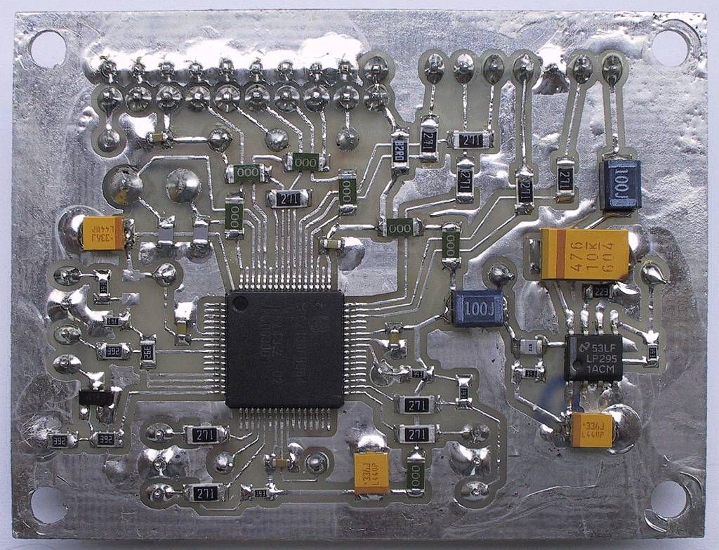
The basic ATNC is based on the LPC2138/01 (or LPC2148) microcontroller:
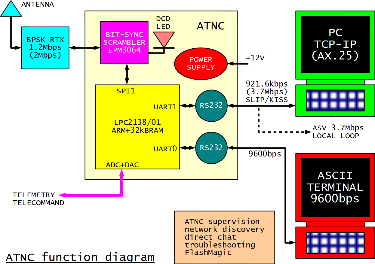
The HDLC controller is implemented in software and is available through the SPI1 peripheral. UART1 is used for high-speed wire communication. The built-in A/D converter is available for telemetry, while a single output pin is available for telecommand. Finally, UART0 is used for system supervision including firmware programming into the built-in FLASH memory.
The ATNC supports three different modes of operation:
(1) simple KISS mode on UART1 (protocol-transparent), compatible with AX.25 software,
(2) NBP user mode running SLIP on UART1 including emulation of Hayes-modem "AT" commands for compatibility with Win98, WinXP and all versions of Linux and
(3) NBP node mode (Advanced SuperVozelj) running NBP local wire loop on UART1.
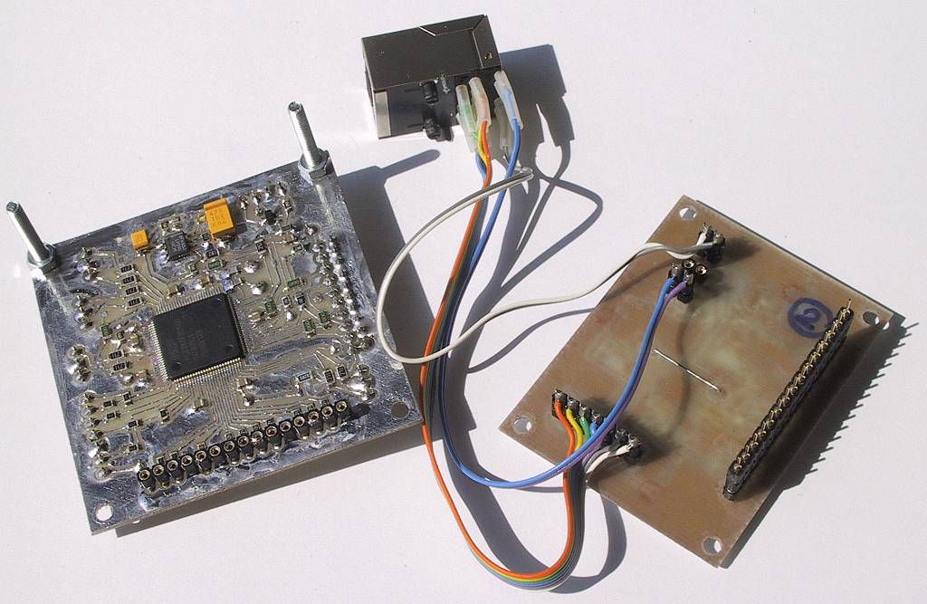
The LPC2138 is soldered onto a simple printed-circuit board:
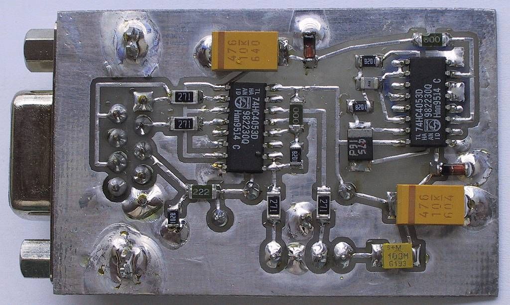
A simple serial interface with two 74HC4053 analog switches is fully RS-232 compatible and works reliably beyond 5Mbps over moderate cable lengths up to 3m:
The first three ATNC prototypes use the bit synchronizers and scramblers developed for the SuperVozelj project many years ago:
The final version of the ATNC uses a much improved bit synchronizer and scrambler, programmed into a single CPLD EPM3064ATC44 (64 macrocells) manufactured by Atlera:
The complete ATNC including a 5V supply regulator is installed in a box 120mm wide, 120mm deep and 30mm high:
The front-panel connectors include the BPSK RTX connector (DIN), the 12V supply connector, the 9600bps RS-232 for supervision (first DB9) and fast RS-232 for data (second DB9):
A much more detailed description of the ATNC including all circuit diagrams is available in the following PDF document. The corresponding design files including printed-circuit boards and firmware (both ASM source and HEX) are included in the following ZIP archive:
ATNC description (SLO)
 ATNC files
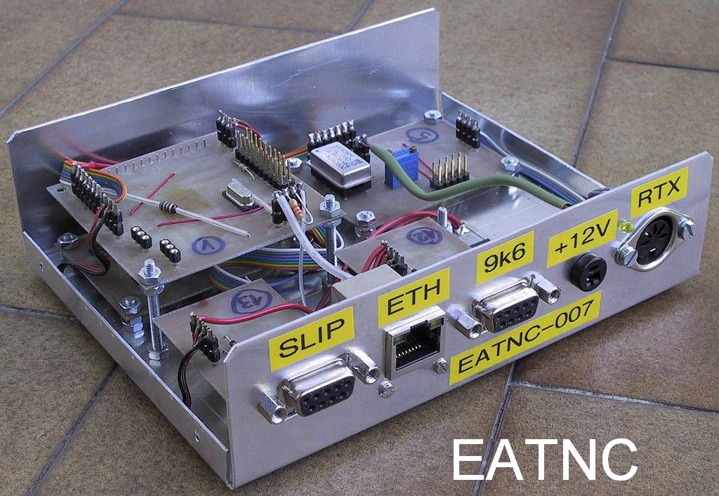
3. EATNC
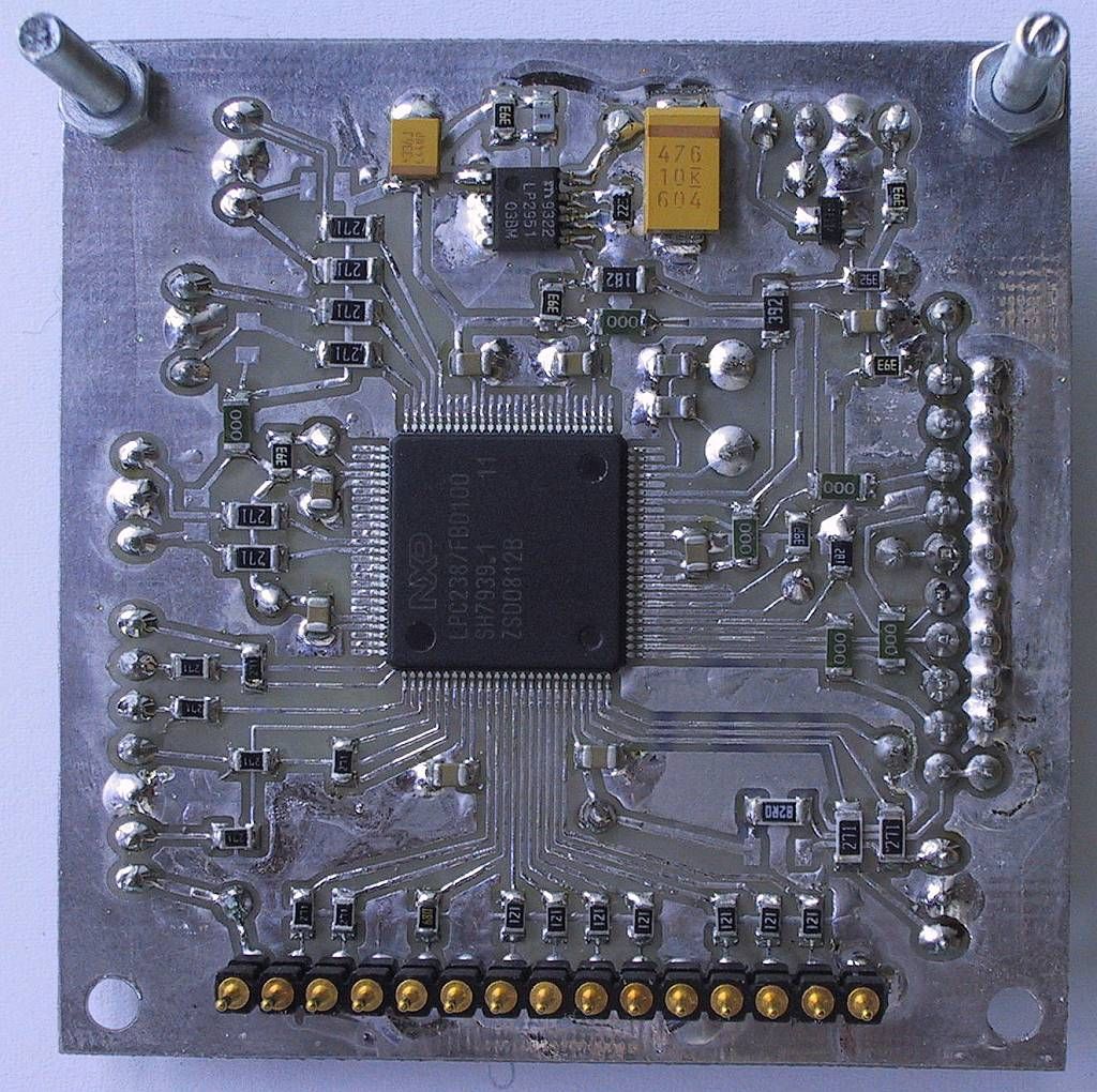
The EATNC is based on the LPC2387 (or LPC2368) microcontroller:
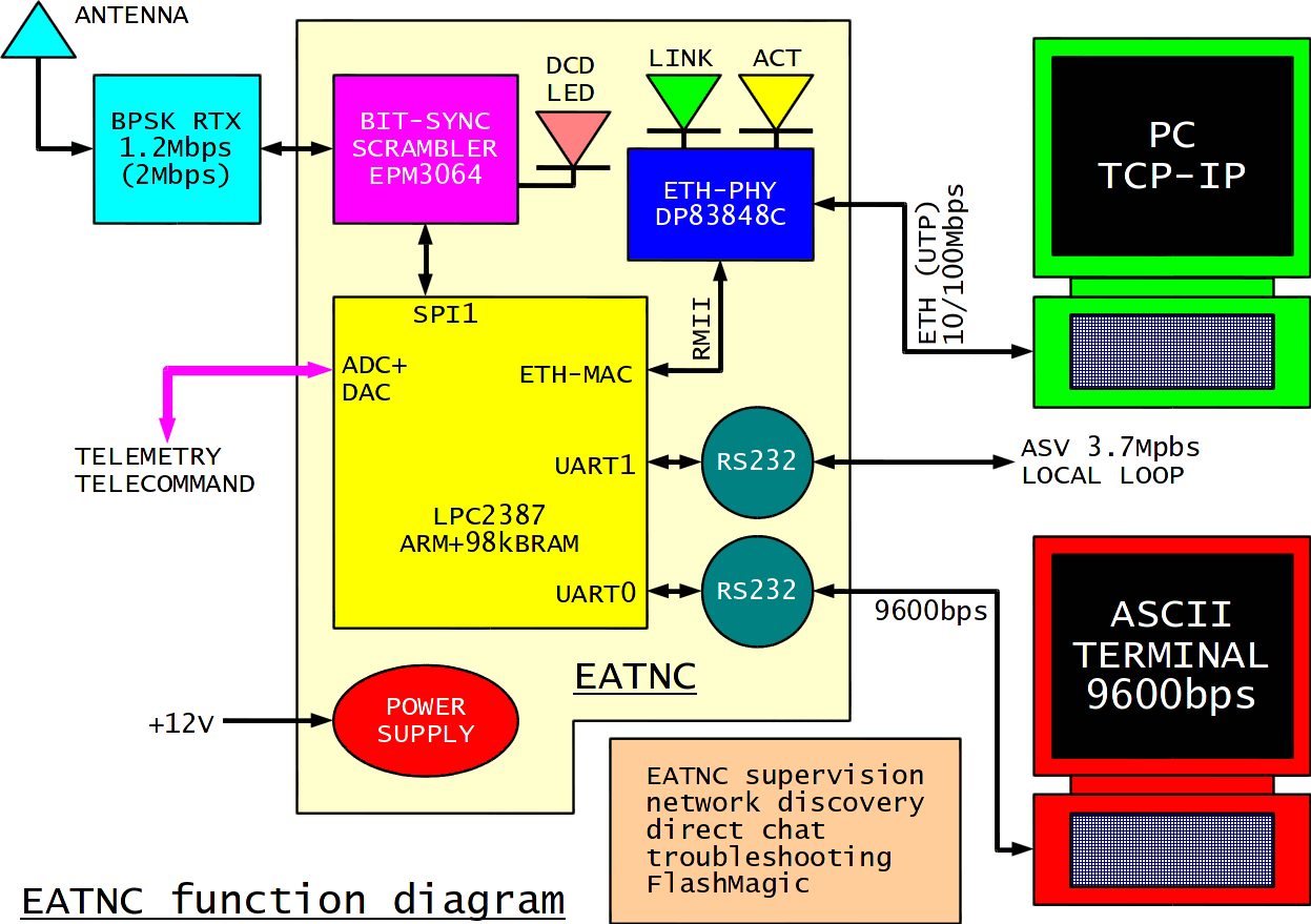
In addition to the ATNC peripherals, the EATNC includes a 10Mbps/100Mbps Ethernet port. The latter supports Auto-Negotiation and Auto-MDIX.
The EATNC supports four different modes of operation:
(1) simple KISS mode on UART1 (protocol-transparent), compatible with AX.25 software (same as ATNC),
(2) NBP user mode running SLIP on UART1 including emulation for Hayes-modem "AT" commands for compatibility with Win98, WinXP and all versions of Linux (same as ATNC),
(3) NBP user mode running IP4 traffic on the Ethernet port and at the same time NBP node mode (Advanced SuperVozelj) running NBP local wire loop on UART1 and
(4) IP4 Ethernet-SLIP converter (radio off, NBP off).
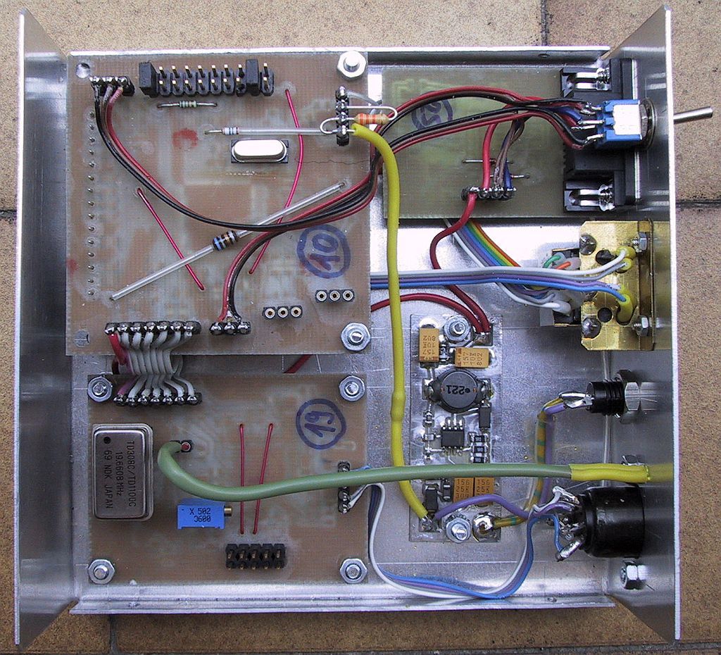
The LPC2138 is soldered onto a simple printed-circuit board:
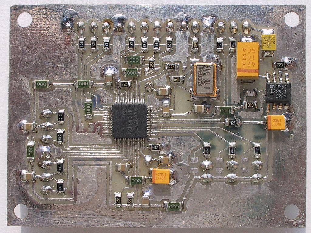
The LPC2387 only contains the Ethernet MAC (digital part). The Ethernet PHY (wire modem) has to be added externally. The DP83848C Ethernet PHY in the EATNC is installed on its own printed-circuit board that can be stacked below the LPC2387 board:
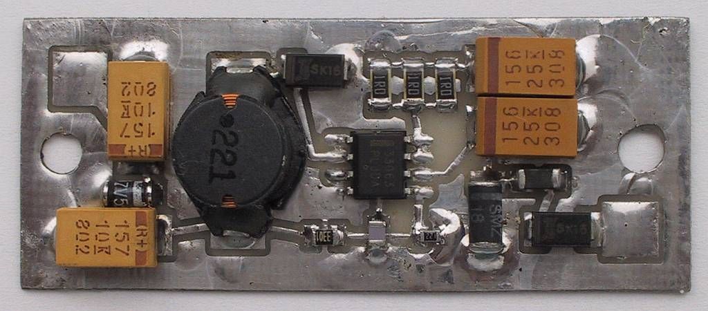
To limit power consumption and heating a switching regulator is recommended in the EATNC:
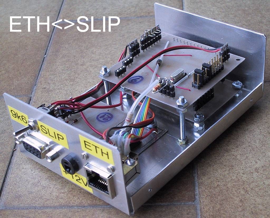
The EATNC can be built with all available ports (width 150mm, depth 120mm and height 40mm):
A DPDT switch can save one RS-232 interface:
A bare Ethernet-SLIP converter does not require the bit-synchronizer-and-scrambler unit nor the radio (DIN) connector.
A much more detailed description of the EATNC including all circuit diagrams is available in the following PDF document. The corresponding design files including printed-circuit boards and firmware (both ASM source and HEX) are included in the following ZIP archive:
EATNC description (SLO)
EATNC files4. MATNC
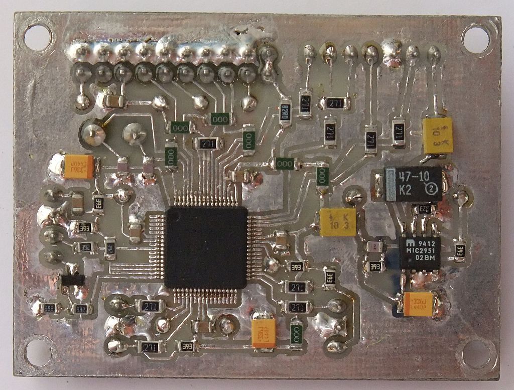
The MATNC is based on the LPC2138/01 (new version with updated A/D converter) or the LPC2148 microcontroller:
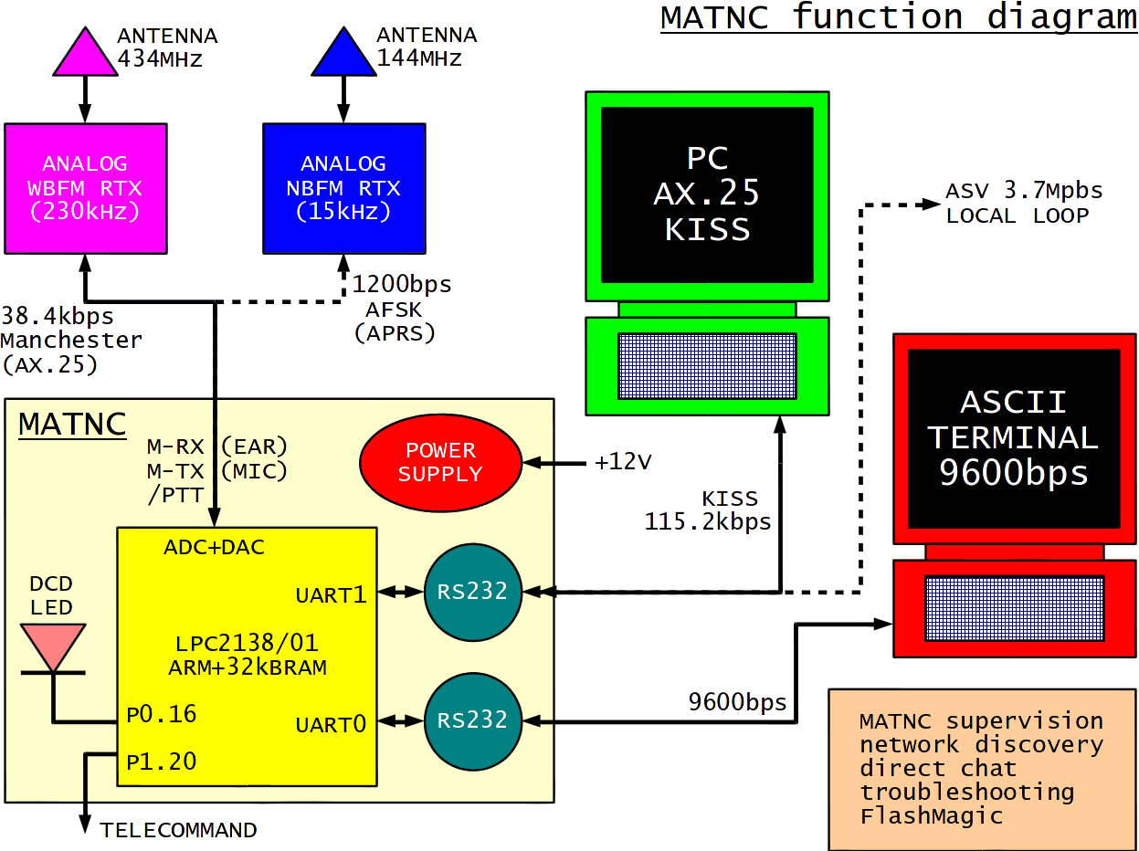
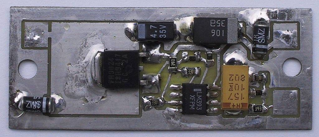
The HDLC controller is implemented in software and is connected to a DSP modem available through the built-in A/D and D/A converters. UART1 is used for high-speed wire communication. A single output pin is available for telecommand. Finally, UART0 is used for system supervision including firmware programming into the built-in FLASH memory.
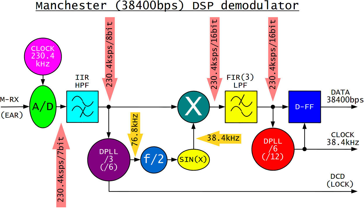
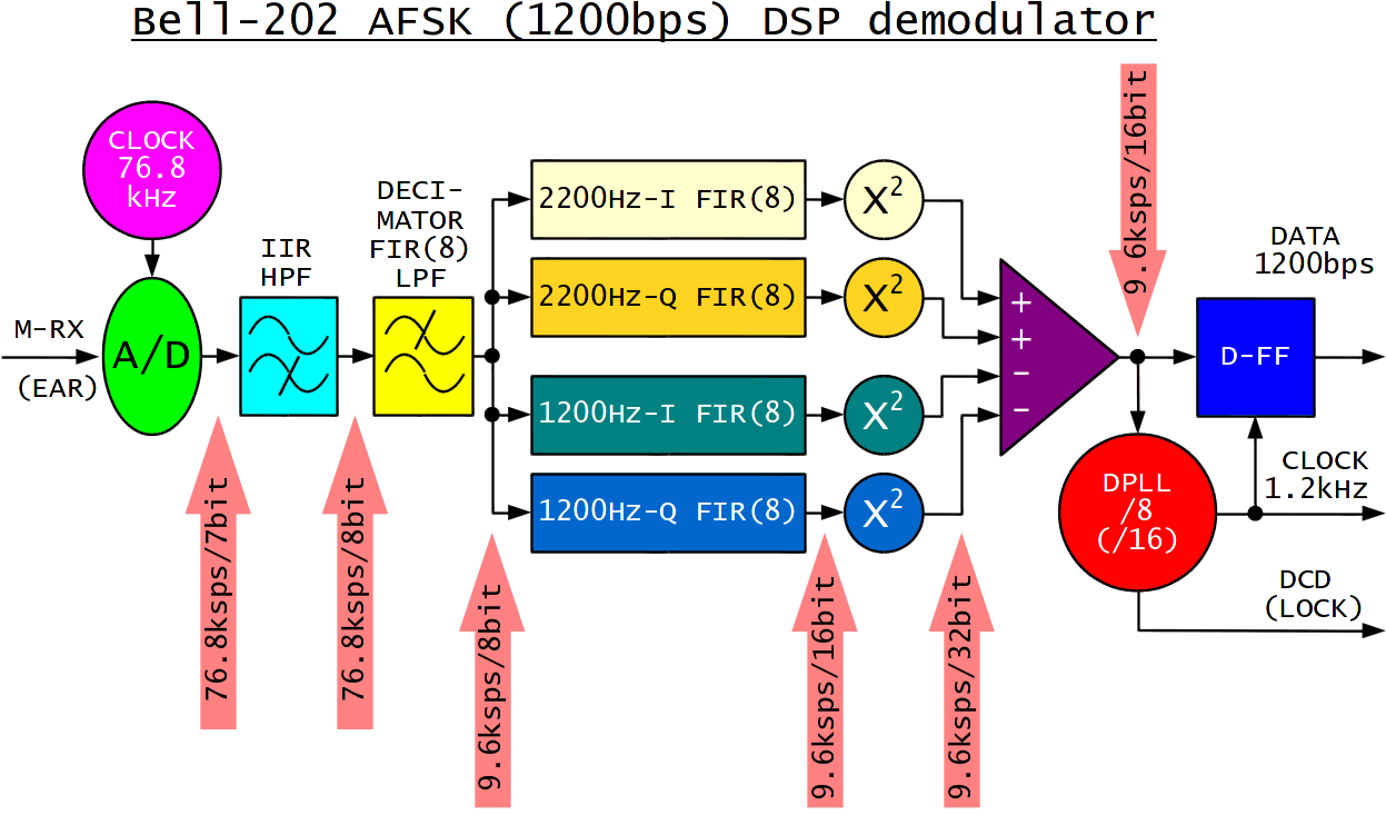
The current firmware supports Manchester and AFSK DSP modems. The Manchester modem can be programmed to operate between 4800bps and 76800bps. The AFSK modem can be programmed to operate between 150bps and 2400bps. At 1200bps the AFSK modem corresponds to the Bell-202 specification using 1200Hz/2200Hz tones.
The MATNC supports four different modes of operation:
(1) simple KISS mode on UART1 (protocol-transparent), compatible with AX.25 software (same as ATNC/EATNC but DSP modem),
(2) NBP user mode running SLIP on UART1 including emulation for Hayes-modem "AT" commands for compatibility with Win98, WinXP and all versions of Linux (same as ATNC/EATNC but DSP modem),
(3) NBP node mode (Advanced SuperVozelj) running NBP local wire loop on UART1 (same as ATNC but DSP modem) and
(4) "inverse" HDLC-KISS mode: AX.25 frames from the analog-radio, DSP-modem port are framed into NBP frames and transmitted to the NBP local wire loop, the reverse also being supported to build AX.25 bridges (APRS data collection, virtual AX.25 nodes etc) through the NBP network.
The printed-circuit board is the same as for the ATNC with just a few components changed:
The Manchester DSP demodulator includes a first DPLL for carrier recovery and a second DPLL for clock recovery:
The AFSK DSP demodulator includes four FIR filters for 1200Hz/2200Hz, I/Q:
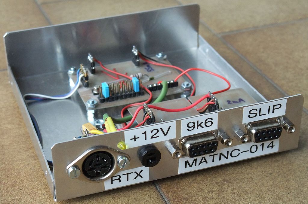
The complete MATNC including a 5V supply regulator is installed in a box 120mm wide, 120mm deep and 30mm high (same as ATNC):
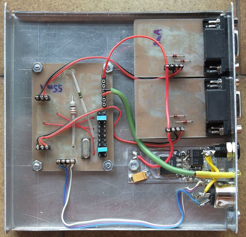
The front-panel connectors include the analog RTX connector (DIN), the 12V supply connector, the 9600bps RS-232 for supervision (first DB9) and fast RS-232 for data (second DB9):
A much more detailed description of the MATNC including all circuit diagrams is available in the following PDF document. The corresponding design files including printed-circuit boards and firmware (both ASM source and HEX) are included in the following ZIP archive:
MATNC description (SLO)
MATNC files5. ASV
The firmware of the ATNC family already supports the operation of multiple ATNCs, EATNCs and MATNCs in a NBP local wire loop of an ASV (Advanced SuperVozelj or Arm SuperVozelj) packet-radio node. An ASV network node for home or office use (gateways!) can therefore be simply assembled from the building blocks presented above.
On the other hand, a mountain-top ASV node has additional requirements. Telemetry of key parameters like receiver AGC, supply voltage or hardware temperature is required. Remote node-reset telecommand is a must, especially if less reliable equipment like IP routers, WLAN (WiFi) equipment or IP cameras is also used. Finally, it makes sense to combine more than one ATNC, EATNC or MATNC in a single package to save connectors and space.
Operating experience with SuperVozelj nodes shows that processor reset is frequently not enough. A lightning strike may trigger a CMOS latch-up and the latter can only be resolved by power cycling if hopefully the hardware survived. A special circuit to remove and reapply +12V power to the whole node while being driven by the ATNC telecommand is required:
How many ATNCs, EATNCs or MATNCs does it make sense to combine in a single package to save connectors and/or space on one side and allow flexibility for node growth and maintenance on the other side? Practical experience shows that it makes sense to package two or three (X)ATNCs together.
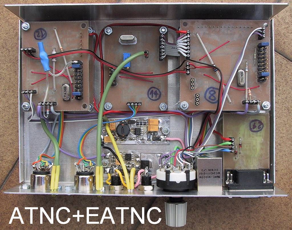
The core of an ASV node is usually formed by an ATNC+EATNC combination. The latter includes the +12V remote-reset circuitry and simple telemetry for the temperature (thermistor) and supply voltage (resistive divider):
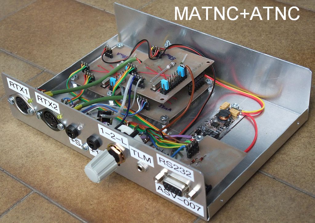
Additional NBP channels require additional ATNCs. AX.25 gateways require additional MATNCs. Another practical combination is a MATNC+ATNC assembly. The latter includes an additional +12V supply switch and a connector for external telemetry:
Many practical hints and connection diagrams for ASV nodes are available in the following PDF document, including a revised design of the bit synchronizer and scrambler. The corresponding design files including printed-circuit boards and firmware (both ASM source and HEX) are included in the following ZIP archive:
ASV description (SLO)
ASV filesAs an example, the packet-radio node S55YNG currently (summer 2012) operates both as an AX.25 node and as a NBP node on the following frequencies:
144.800MHz 1200bps APRS RX connected to both the SuperVozelj and a MATNC in parallel,
430.80MHz 1.2288Mbps BPSK ZIF RTX connected to both the SuperVozelj and an ATNC in parallel,
434.10MHz 38.4kbps Manchester/WBFM RTX connected to the SuperVozelj only,
1293.00MHz 38.4kbps Manchester/WBFM RTX connected to the SuperVozelj only,
1298.68MHz 1.2288Mbps BPSK ZIF-RTX connected to an ATNC only and
2360.00MHz 1.2288Mbps/2Mbps BPSK RTX+transverter connected to the SuperVozelj, to an ATNC and to an EATNC (two different data rates for NBP) all in parallel.
Finally, another MATNC is programmed for 38.4kbps Manchester and is connected by wire (no radio) to an 38.4kbps port of the SuperVozelj node forming an AX.25-NBP gateway. Although a WLAN (WiFi) router and an IP camera are planned, there is no Ethernet equipment on S55YNG yet and the Ethernet port is only used for service.
All radio equipment of S55YNG is shown on the following photo:
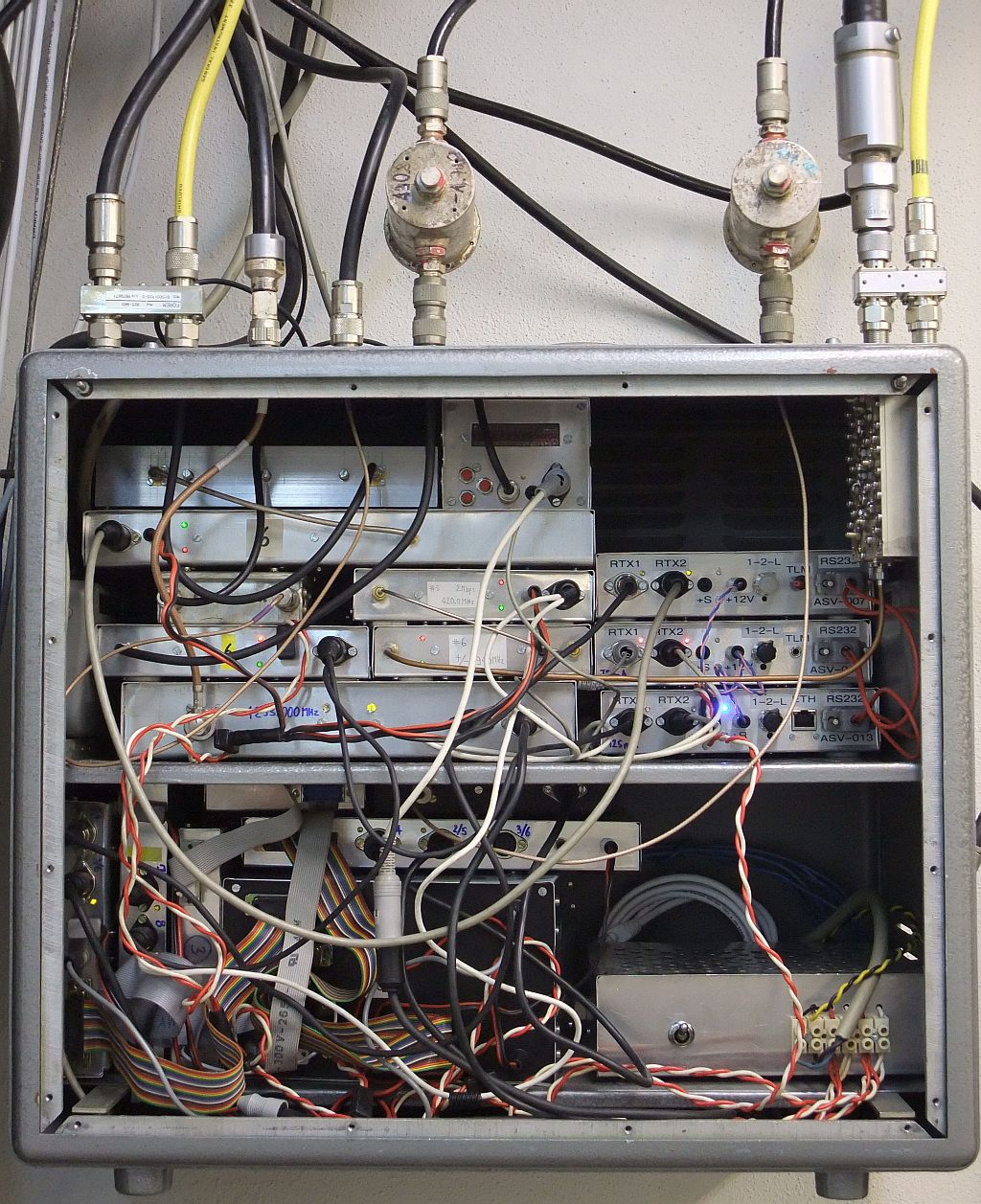
Cavity filters above and in the upper part of the cabinet. Radio transceivers in the upper left side of the cabinet. NBP equipment in the upper right side of the cabinet. AX.25 SuperVozelj node in the lower left side of the cabinet. 12V power supply in the lower right side of the cabinet.
6. RATNC
The RATNC is based on the LPC2387 (or LPC2368 or LPC2378 or LPC2388) microcontroller:
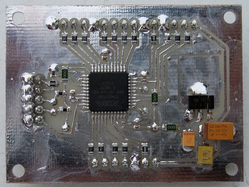
The RMII-HDLC converter is programmed into a single CPLD EPM3032ATC44 (32 macrocells) manufactured by Atlera. The printed-circuit board has the same size and shape as the DP83848C Ethernet PHY (EATNC) that can be stacked below the LPC2387 board:
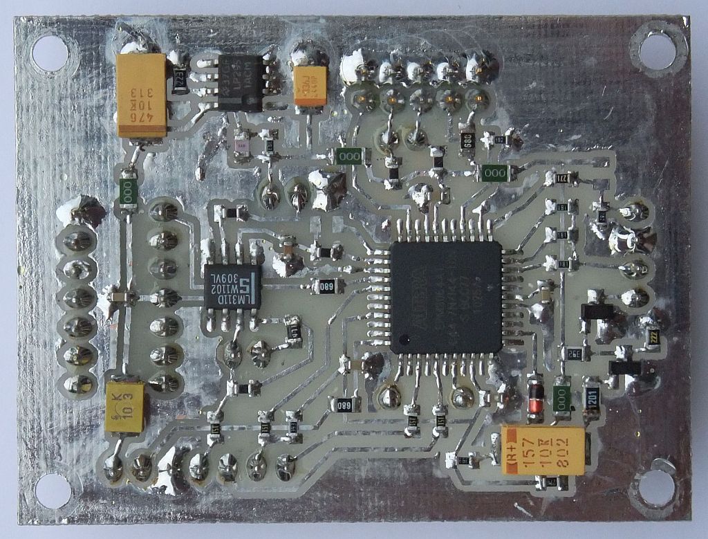
The RATNC uses a bit synhronizer and scrambler, programmed into a single CPLD EPM3064ATC44 (64 macrocells) manufactured by Atlera, operating at 8-times the data rate (80MHz for 10Mbps):
New, compatible and interchangeable printed-circuit boards have been developed for both the 100-pin microcontrollers LPC2368 and LPC2387 and the 144-pin microcontrollers LPC2378 and LPC2388:
The complete RATNC including a switching 5V supply regulator is installed in a box 120mm wide, 120mm deep and 40mm high:
The front-panel connectors include the BPSK RTX connector (DIN), the 12V supply connector, the 9600bps RS-232 for supervision (first DB9) and fast RS-232 for data (second DB9):
A much more detailed description of the RATNC including all circuit diagrams is available in the following PDF document. The corresponding design files including printed-circuit boards and firmware (both ASM source and HEX) are included in the following ZIP archive:
RATNC description (SLO)
RATNC files7. SATNC
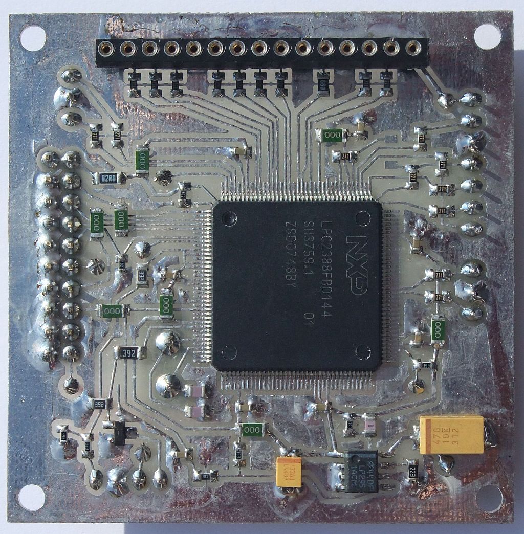
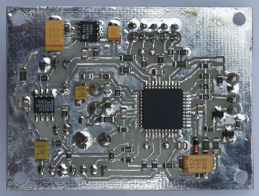
The SATNC is based on the LPC2387 (or LPC2368 or LPC2378 or LPC2388) microcontroller:
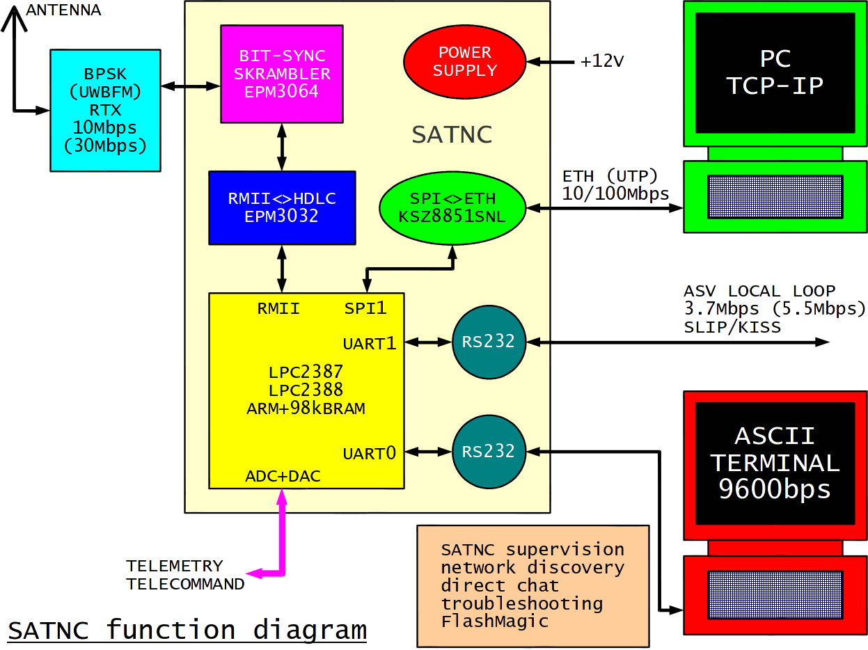
The additional 10Mbps/100Mbps Ethernet communication port is built around the KSZ8851SNL chip and connected to the available SPI port of the microcontroller. The KSZ8851SNL supports a hardware IEEE 802.3x flow control thus enabling efficient Ethernet commmunication:
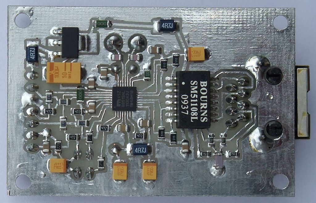
An additional bit synchronizer and scrambler, programmed into a single CPLD EPM3064ATC44 (64 macrocells) manufactured by Atlera, running from a cheaper 40MHz crystal in place of the more expensive 80MHz oscillator for 10Mbps is also available:
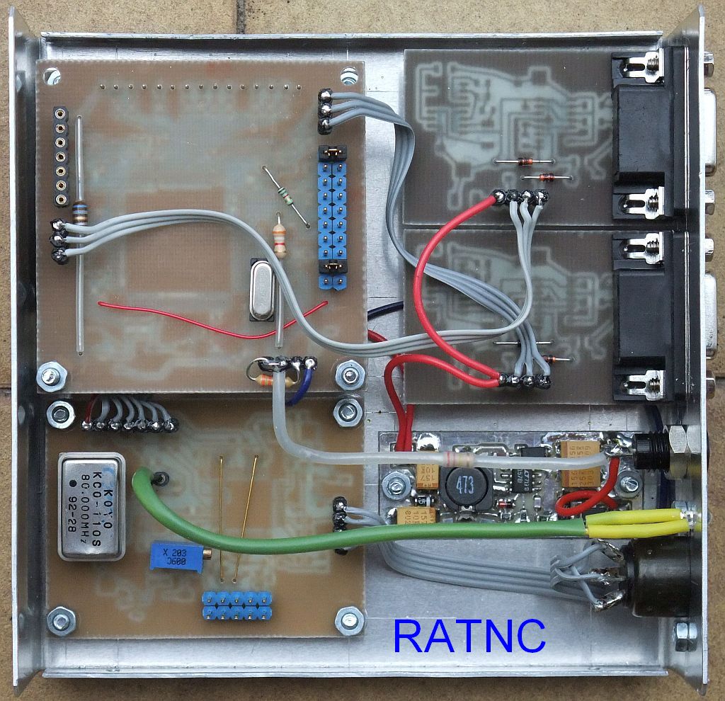
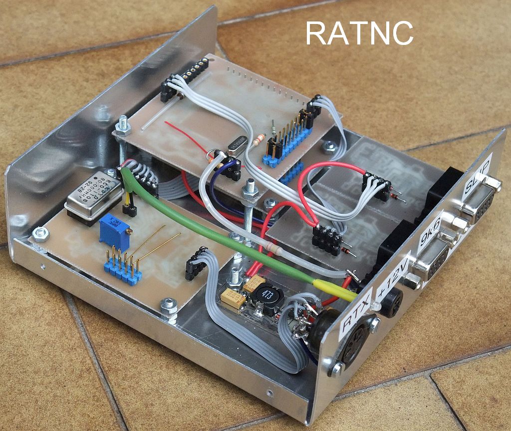
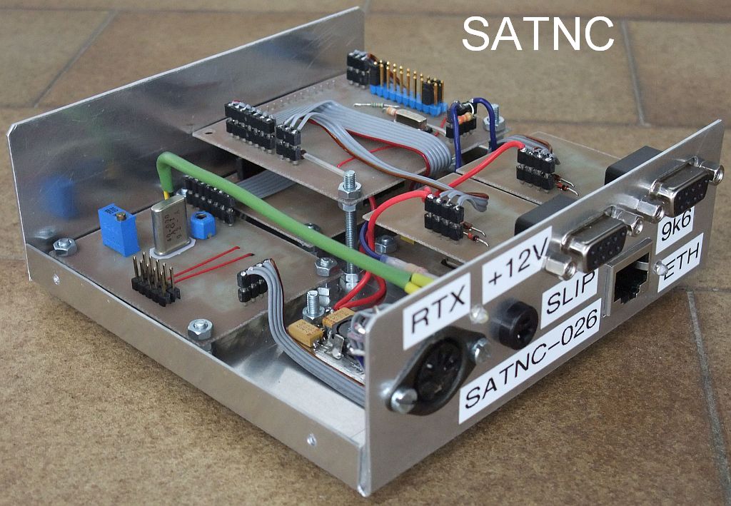
The complete SATNC including a switching 5V supply regulator is installed in a box 120mm wide, 120mm deep and 40mm high. The 80MHz-oscillator version is shown on the following photo:
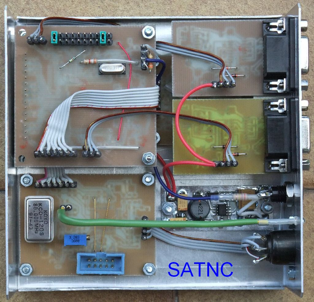
The front-panel connectors include the BPSK RTX connector (DIN), the 12V supply connector, the fast RS-232 for data (first DB9), the RJ45 Ethernet connector and the 9600bps RS-232 for supervision (second DB9). The 40MHz-crystal version is shown on the following photo:
A much more detailed description of the SATNC including all circuit diagrams is available in the following PDF document. The corresponding design files including printed-circuit boards and firmware (both ASM source and HEX) are included in the following ZIP archive:
SATNC description (SLO)
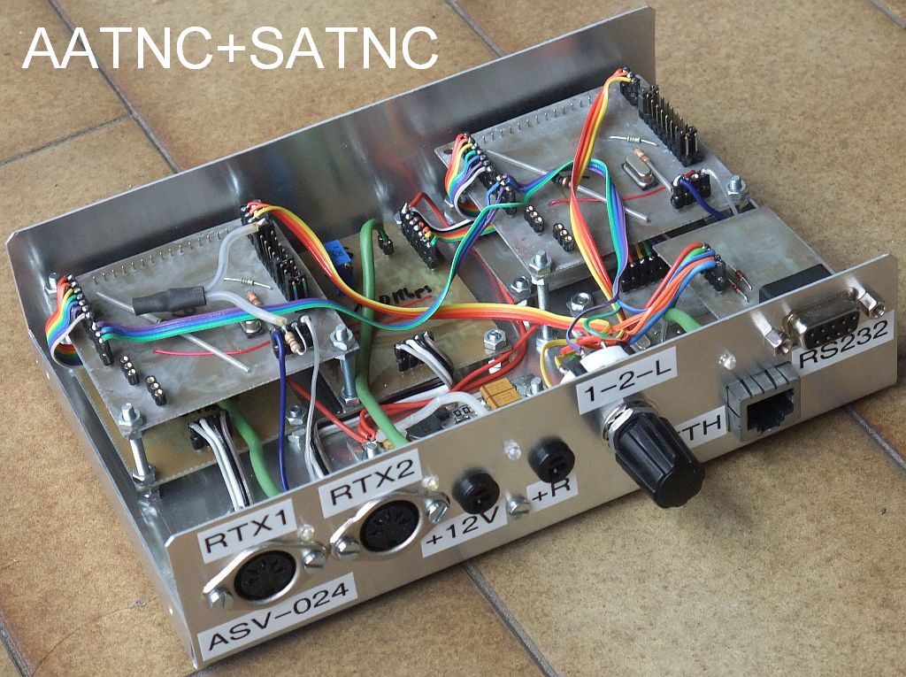
SATNC filesOf course the SATNC is an excellent choice for an ASV node. A very practical combination is an AATNC+SATNC combination built in the same case including the +12V remote-reset circuitry and simple telemetry for the temperature (thermistor) and supply voltage (resistive divider):
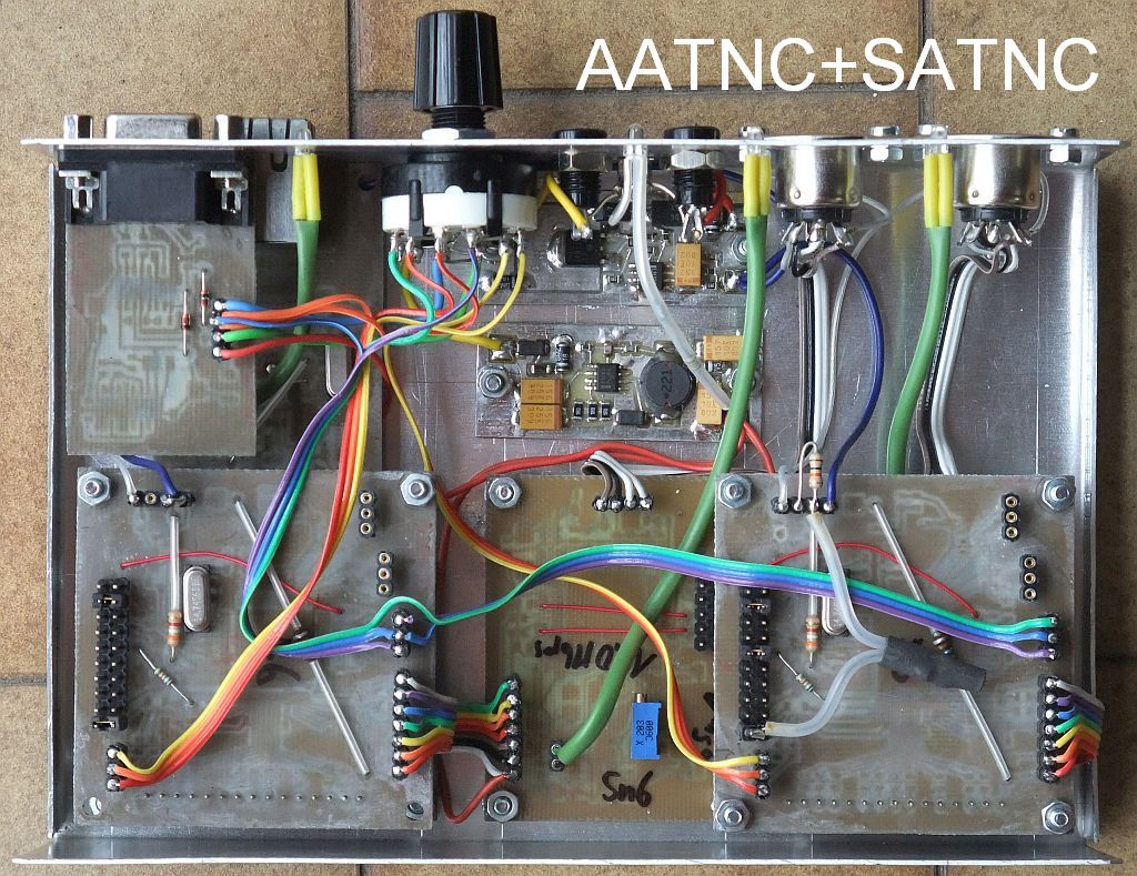
The front-panel connectors include two BPSK RTX connectors (DIN), two 12V supply connectors, in (+12V) and out (+R) to reset other equipment as well, a three-position switch for the RS-232 function (AATNC control, SATNC control and ASV loop), the RJ45 Ethernet connector and the DB9 RS-232 connector. The bit synchronizer and scrambler uses a 80MHz SMD oscillator for 10Mbps:
The RS-232 local loop becomes a bottleneck when two or more RATNCs or SATNCs are interconnected in a single network node. Even clocking the LPC23xx at 88MHz (XTAL*6) and the RS-232 local loop operating at 5.5Mbps the data-transfer rate is limited to about 4Mbps. A more efficient solution is to interconnect two SATNCs using their Ethernet ports.