(THEORY)
(ANALOG)
(DIGITAL)
(SOFTWARE)
(HOME)
A homemade receiver for GPS & GLONASS satellites
Matjaz Vidmar, S53MV (ex YU3UMV, YT3MV)
4. Homemade receiver modules for GPS & GLONASS
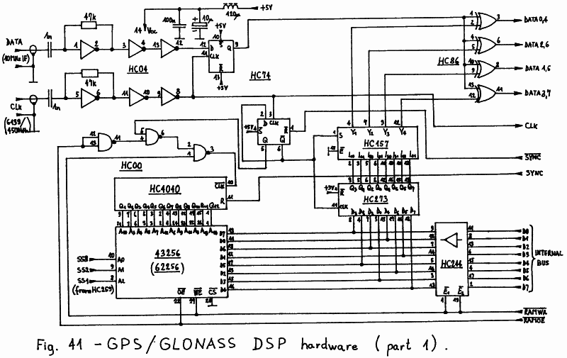
4.10. GPS/GLONASS DSP hardware
The theory of operation of the dedicated GPS/GLONASS DSP
hardware has already been discussed in 3.6. Therefore the
practical implementation will only be described in the
following paragraph.
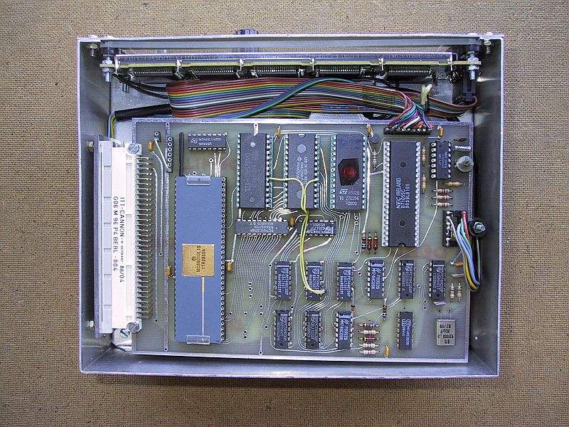
The dedicated GPS/GLONASS DSP hardware is built as a
peripheral plug-in module for the DSP computer [1], [2].
The circuit diagram of the GPS/GLONASS DSP hardware is
shown on Fig. 41 and Fig. 42. The DSP hardware module
includes two amplifiers for the limited IF signal and master
clock coming from the analog part of the GPS or GLONASS
receiver, a look-up table RAM, four signal-despreading
mixers, four correlator counters, all of the timing logic to
scan the look-up table and generate interrupts to the CPU
and all of the interface circuits necessary for the DSP
computer bus.
The input signal amplifiers are built with 74HC04
inverters to amplify the input signals of a few hundred
millivolts up to TTL levels. In this way the signal levels
in the analog part of the GPS or GLONASS receiver can be kept
more than 20dB lower, reducing the shielding requirements.
The supply voltage of the 74HC04 is additionally filtered
to reject the disturbs usually present on the +5V computer
bus power supply. The limited input signal is then sampled by
a D-flip-flop (1/2 74HC74). Considering the relationship
between the IF and the sampling frequency, the sampling
operation also provides a third downconversion.
The look-up tables are stored in a 32kX8 static RAM.
The RAM area is divided into 8 separate areas of 4kbytes
each, selectable through a microprocessor output port. In this
way the look-up table needs not to be rewritten when switching
to another satellite. The receiver is usually time-multiplexed
among four different satellites and all four different look-up
tables are stored in the RAM. When switching to another
satellite, the hardware is simply switched to another look-up
table and this only requires executing a few instructions
instead of rewriting the whole 4kbyte table.
The 4kbytes of each look-up table are written as bytes by
the microprocessor. The microprocessor writes all of the bytes
to the same location, since the address counter is incremented
automatically after each write operation. In read mode the
look-up table is scanned by the same hardware counter
(74HC4040) clocked at half the sampling frequency (3069.5kHz
for GPS or 2250kHz for GLONASS). The byte data is latched
(74HC273) and then multiplexed to 4 bits (74HC157) to get all
of the four required local signal replicas to be multiplied
(EXOR 74HC86) with each input signal sample. Each look-up
table may be thus up to 8192 samples long. The unused samples
need not be written since they are not used by the hardware.
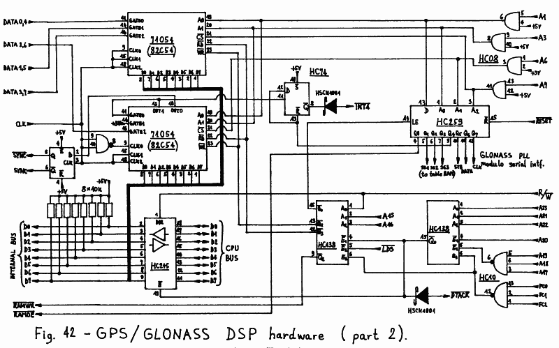
The dedicated DSP hardware requires six programmable
counters: four correlation accumulators, a sampling frequency
divider and a variable delay counter, all contained in two
uPD71054 (82C54) integrated circuits. Each uPD71054 contains
three almost independent 16-bit counters that can be
programmed in different ways. For example, the four
correlation counters are clocked with the same signal sampling
frequency and the signals are fed to the GATE inputs, which
are programmed as clock enables.
The signal sampling frequency (6139 or 4500kHz) is
divided down to 1kHz to match the C/A-code period (1ms). This
signal is also used to request interrupts from the CPU, since
the correlation counters need to be read each millisecond.
After receiving an interrupt request, the CPU will latch
the content of all counters in a single bus operation and then
read the latched content of every single counter in separate
bus operations. The sampling clock divider is also latched and
read and its content is used as an accurate timing reference.
Every interrupt request sets a flip-flop that needs to be
reset by the microprocessor after the interrupt has been
serviced. Interrupt arm (enable) and reset (disable) is
performed through one (Q4) of the eight output-port bits
provided by the 74HC259 addressable latch. Of the remaining
7 bits, three (Q1, Q2 and Q3) are used to select one of the
eight look-up tables in the RAM and another bit (Q0) is used
to select either write or read mode for the look-up table
logic. The last three bits (Q5, Q6 and Q7) are used to
control the GLONASS PLL modulo or as spares in a GPS receiver.
The bus interface to the DSP computer bus includes a
bidirectional data-bus buffer (74HC245) and an address
selection logic (two 74HC138s and 74HC10). The bus interface
does not request any wait states from the MC68010 CPU. The
address decoding for the uPD71054 programmable counters must
allow simultaneous write operations to both control registers
of both peripherals, to be able to latch the content of all
of the counters exactly at the same time. Finally, the RESET
signal is fed to the 74HC259 addressable latch essentially
to prevent any interrupts or other unintended operations
before the whole DSP hardware is correctly initialized.
The bus addresses are assigned as follows:
$E0001   - Disable look-up table write mode
$E0003   - Enable look-up table write mode

$E0009   - Look-up table address A2 reset
$E000B   - Look-up table address A2 set
$E0041   - Look-up table address A1 reset
$E0043   - Look-up table address A1 set
$E0049   - Look-up table address A0 reset
$E004B   - Look-up table address A0 set

$E0081   - Reset & disable 1ms interrupt
$E0083   - Enable 1ms interrupt
$E0082   - Reset & enable 1ms interrupt, long transfer!

$E0089   - GLONASS PLL modulo STROBE reset
$E008B   - GLONASS PLL modulo STROBE set
$E00C1   - GLONASS PLL modulo DATA reset
$E00C3   - GLONASS PLL modulo DATA set
$E00C9   - GLONASS PLL modulo CLOCK reset
$E00CB   - GLONASS PLL modulo CLOCK set

$E800B   - Common WRITE to both 71054 command registers

$E8041   - 71054 #1 CTR0 - data 0,4 accumulator
$E8043   - 71054 #1 CTR1 - data 1,5 accumulator
$E8049   - 71054 #1 CTR2 - data 3,7 accumulator
$E804B   - 71054 #1 command register

$E8081   - 71054 #2 CTR0 - variable C/A-code delay
$E8083   - 71054 #2 CTR1 - GPS /6139 or GLONASS /4500 clk
$E8089   - 71054 #2 CTR2 - data 2,6 accumulator
$E808B   - 71054 #2 command register

$F8001   - WRITE byte to look-up table
However, one should notice that the remaining addresses in the range from $E0000 to $FFFFF are not fully or correctly decoded, although the module will acknowledge the access to the MC68010. Accessing other addresses in this range (either reading from or writing to) will probably cause an erratic operation of the module. The 74HC259 addressable latch is programmed by writing to the specified locations. Since only the address is important and the data is ignored, CLR.B instructions are used to write to single bytes and a CLR.L instruction is used to reset and arm the interrupt flip-flop.
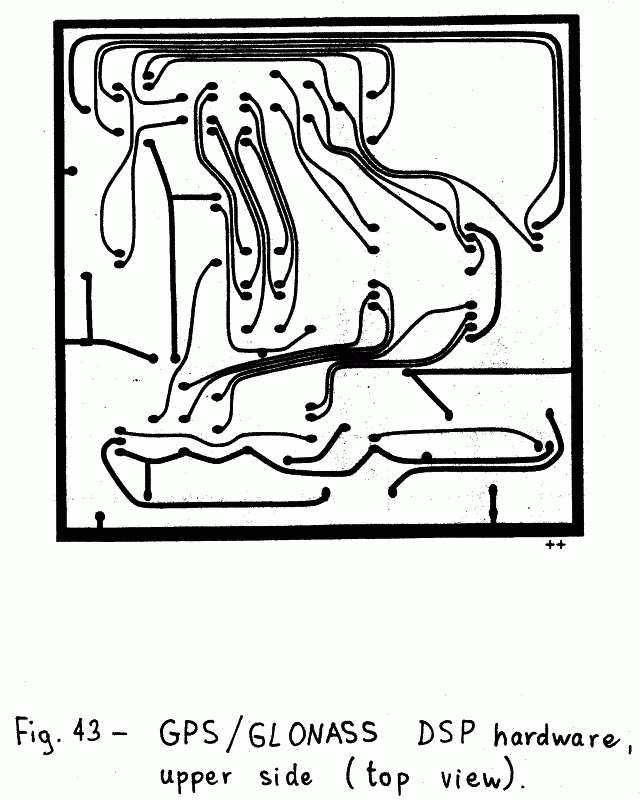
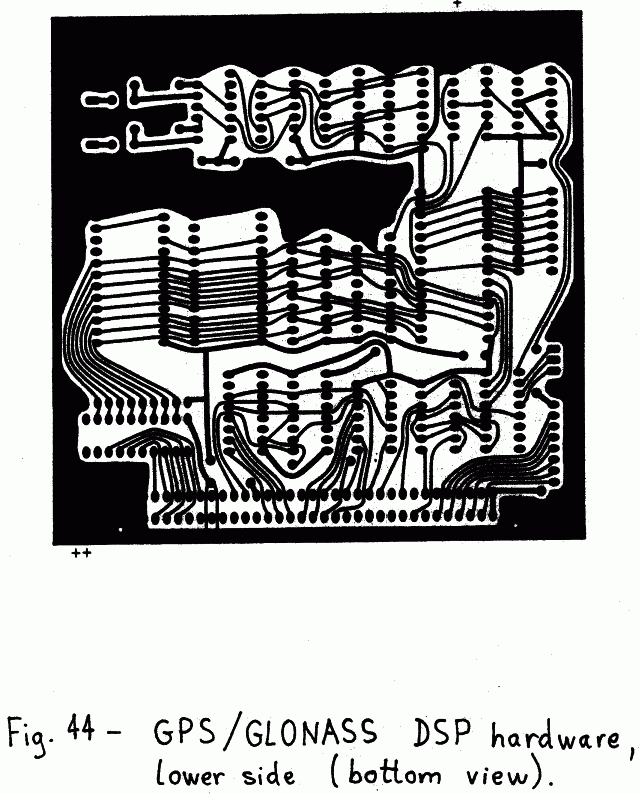
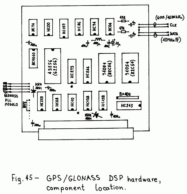
The dedicated DSP hardware module is built on a double-sided printed-circuit board as shown on Fig. 43 and Fig. 44. The location of the components is shown on Fig. 45. The single resistors, diodes and the 100uH choke are installed horizontally. The eight 10kohm resistors are in a single 9-pin SIL package. The capacitors are ceramic except the 10uF "tantalum drop" and all have a pin spacing of 5mm.
The 74HC4040 should NOT be replaced by a standard 4040
device, since the latter is too slow for a correct operation
in the described circuit. To allow an eventual troubleshooting
it is recommended to install at least the two 71054 counters
and the 43256 RAM on good-quality sockets. The speed of the
RAM is unimportant, since even the slowest 150ns static RAMs
are fast enough for this project.
The dedicated DSP hardware module is inserted in the DSP
computer bus with a 64-pole "eurocard a+c" connector. The
remaining connectors include a 5-pin socket for the input IF
signal and clock, a 4-pin socket for the GLONASS PLL modulo
control and a 8-pin socket for the interrupt selection. All
of these are made from parts of good-quality IC sockets.
The dedicated DSP hardware module only includes logic
circuits that require no alignments.
4.11. GPS/GLONASS portable receiver CPU
The described GPS or GLONASS receiver can be built as an
interface for the DSP computer [1] and [2] or as a
stand-alone, portable receiver. In the latter case the
receiver needs its own microcomputer with a keyboard and a
LCD display. After considering several possible alternatives,
the simplest solution resulted in using a suitably modified
CPU board as described in [1] and [2] as the microcomputer.
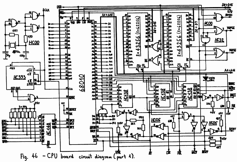
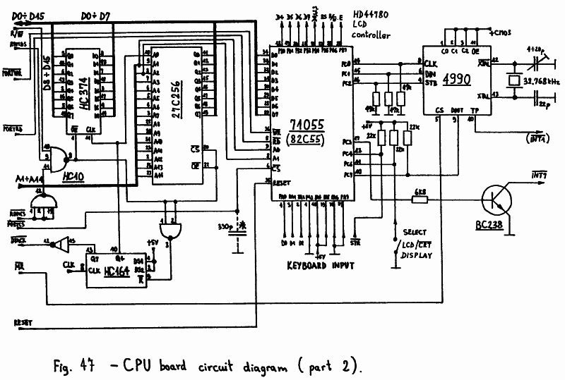
The circuit diagram of the modified CPU board is shown on Fig. 46 and Fig. 47. Since a GPS or GLONASS receiver is a portable device, the power consumption is important and 74HCxx logic devices should be used everywhere. This allows to omit three 3.3kohm pull-up resistors. The original DSP computer CPU board requires the following modifications:
(1) The pads below the EPROM socket should be connected so
    that pin 27 receives the A14 signal required by the
    27C256 EPROM. Originally this pin is connected to +5V,
    using a 27128 EPROM.
(2) The RAM should be increased from 64kbytes up to 128kbytes.
    This is achieved by piggy-back soldering two additional
    43256 RAM chips on top of the existing two RAM chips on
    CPU board. All pins of the additional RAMs are connected
    in parallel with the existing RAM pins except for pin 20
    (chip select). The two chip-select pins of the added RAM
    chips are then wired to pin 11 (Q4) of the middle 74HC138
    address decoder.
(3) A HSCH1001 Schottky diode should be connected between
    pin 11 (Q4) of the top 74HC138 address decoder and the
    DTACK signal (pin 12 of the 74HC05), to acknowledge the
    additional RAM chips to the CPU.
The keyboard connection remains unchanged. The total/partial
reset switch has a new function with the GPS or GLONASS
software. In the case of a stand-alone, portable receiver,
this input should always be left open (+5V)!
The parallel output port (uPD71055 channel B) is now used
to command the HD44780 LCD controller. Since there are only
8 output bits available, the HD44780 is driven in the 4-bit
mode, write only. The real-time clock chip uPD4990 is required
by the GPS or GLONASS software and must remain in place.
The INT7 jumper must remain in place for keyboard interrupt
requests while the INT1 jumper is no longer needed, although
it may remain in place.
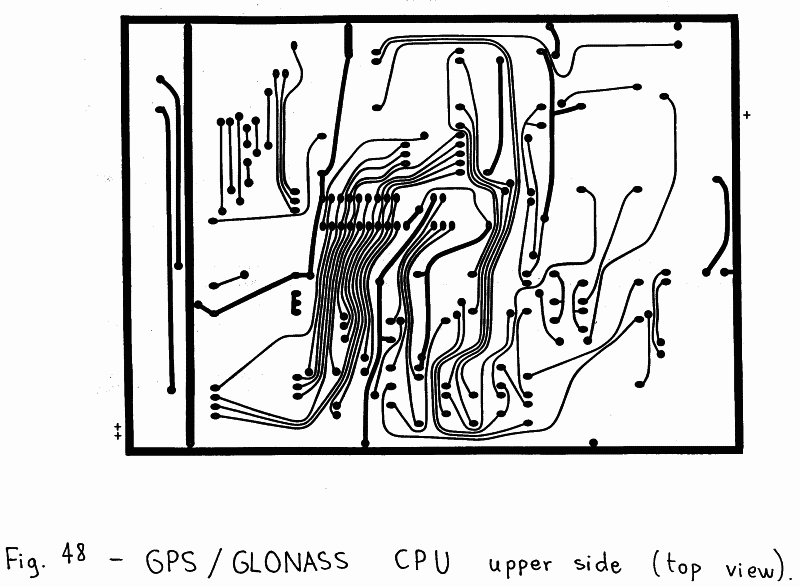
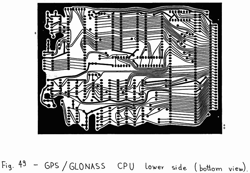
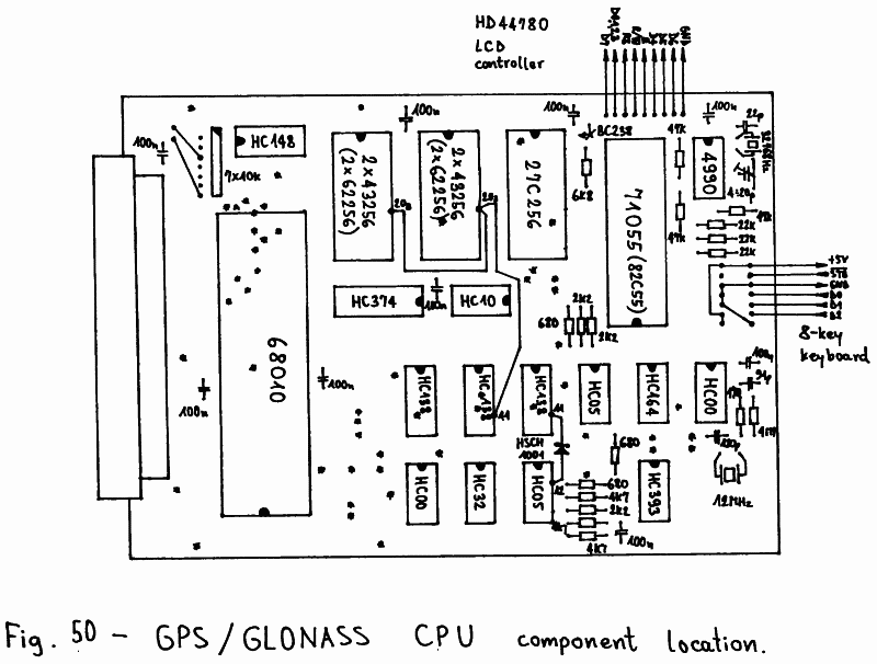
The printed circuit board is not modified, as shown on Fig. 48 and Fig. 49. The additions and modifications are well visible on the component location plan on Fig. 50. The connections of the 8-key keyboard and of the LCD controller are also shown on Fig. 50.
It is recommended that the CPU board is tested first,
if possible, in a DSP computer and the described modifications
are only applied to a 100% tested and working CPU board.
In particular, the CPU board should be tested at higher clock
frequencies to find any defective components. A 10MHz version
of the MC68010 will usually work up to 15MHz clock frequency
at room temperature, so a 12MHz clock crystal is a safe
choice. The GPS or GLONASS software does not require such a
high clock frequency, but the accuracy of some measurements
is higher and the updating of the display is faster at higher
clock rates.
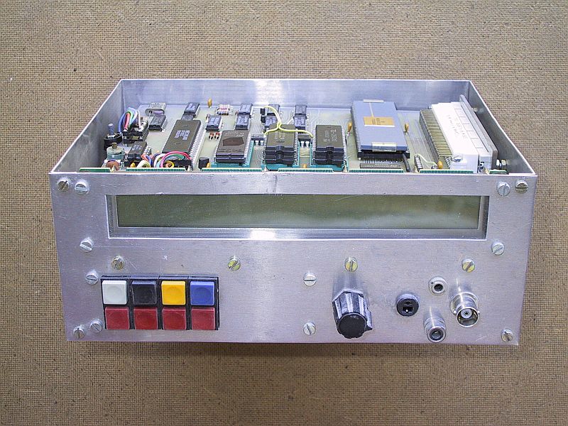
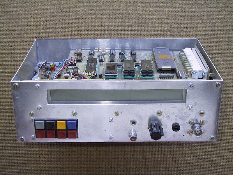
4.12. 8-key keyboard
A portable GPS/GLONASS receiver requires a small keyboard
to issue commands to the computer. Since a full ASCII keyboard
is unpractical for a portable piece of equipment, a small
8-key keyboard was developed for portable receivers.
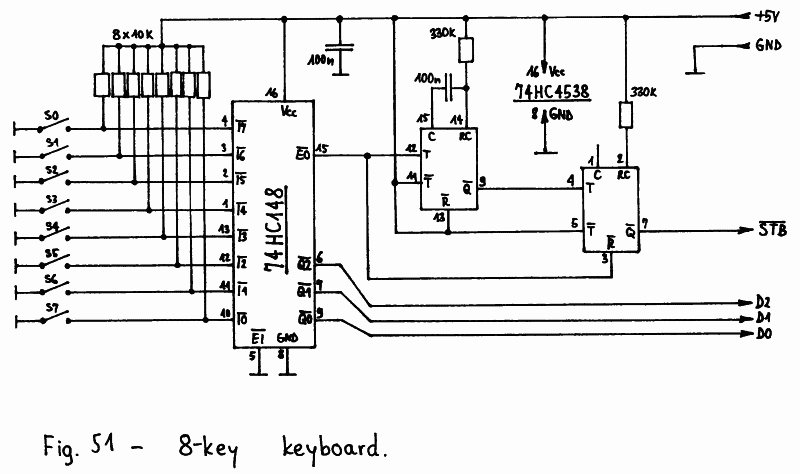
The circuit diagram of the 8-key keyboard is shown on Fig. 51. The 8 keys close towards ground, otherwise the input lines are held high by pull-up resistors. A priority encoder (74HC148) is used to encode the 8 keys into 3 bits. A double monostable (74HC4538) is used to generate the strobe pulse after a key is depressed.
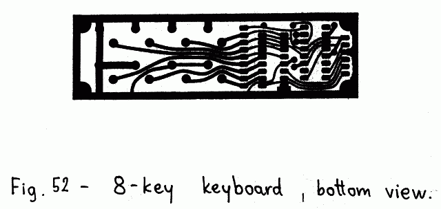
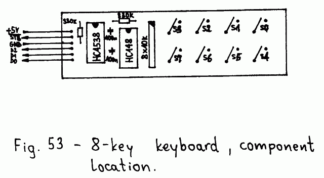
The 8-key keyboard is assembled on a small single-sided printed circuit board shown on Fig. 52. This printed circuit board was designed to fit on the front panel of the receiver and carry eight square (12.7mmX12.7mm) pushbuttons. The location of the components is shown on Fig. 53. Due to the space constraints all of the components should have a low profile and small dimensions. The capacitors have a 2.5mm pin spacing and the resistors are installed horizontally. The eight 10kohm resistor network in a SIL package should be first soldered in place and then bent towards the circuit board. The 6-pin connector is installed on the back - solder side of the board!
The GPS/GLONASS receiver software only accepts ASCII
characters from $30 to $37 as commands, corresponding to
numerals 0 to 7. These can be generated by a standard ASCII
keyboard with a parallel output or by suitably wiring the
described 8-key keyboard. In particular, to obtain the
codes between $30 and $37, the outputs D0, D1 and D2 should
be wired to the corresponding inputs on the CPU board.
In addition, D3, D6 and D7 should be connected to ground and
D4 and D5 to +5V. All these connections, including the supply
rails and the strobe signal, were already shown on Fig. 50.
4.13 LCD display module
The only practical display for a portable GPS/GLONASS
receiver is a LCD module with built-in drivers. Such modules
are available in many different sizes and shapes and may
or may not be equipped with a display controller. LCD modules
with a built-in controller are easy to use, since the
interfacing to any microprocessor is very simple: it is
identical to a parallel I/O port.
Most small dot-matrix alphanumeric LCD modules use the
Hitachi HD44780 LCD controller. This integrated circuit has a
built-in, extended ASCII character generator, a display
area RAM including up to two rows of 40 characters each and
all of the timing circuits to drive the LCD. Modules using the
HD44780 controller may have a different number of characters
per row or rows displayed, the total number of characters is
however limited by the internal RAM to 80. Since the HD44780
SMD flat package has only 80 pins, additional LCD driver chips
(HD44100) are used in most LCD modules.
A LCD module with two lines of 40 ASCII characters each
was selected for the described GPS/GLONASS receiver. Such
a LCD module includes the liquid-crystal display itself,
one HD44780 LCD controller and four HD44100 LCD drivers.
Further, the display module may include some form of
illuminating the LCD, either EL foil or LED. The latter
is recommended if the GPS/GLONASS receiver is to be used at
night as well.
Although such display modules are available from several
different manufacturers, they all have the same dimensions
of the carrier printed circuit board: 182mm(width)X
X33.5mm(height)X13mm(thickness) and the same 14-pin electrical
connector. The pin numbers are usually marked on the
printed-circuit board and the pin allocations are as follows:
pin  1    Vss    Ground
pin  2    Vdd    +5V supply
pin  3    Vo     LCD voltage, tap of the contrast control pot
pin  4    RS     Register Select, 0=instruction, 1=data
pin  5    R/W    Read/Write, 0=write, 1=read
pin  6    E      Enable, 0=inactive, 1=active
pin  7    DB0    LSB data, 8-bit bus
pin  8    DB1
pin  9    DB2
pin 10    DB3
pin 11    DB4    LSB data, 4-bit bus
pin 12    DB5
pin 13    DB6
pin 14    DB7    MSB data
EL or LED backlight may have two additional pins on the
connector or solder pads on the printed-circuit board.
When LCDs are driven in time multiplex, the adjustment
of the voltage applied to the LCD is critical to obtain
a good contrast. A contrast control potentiometer is
usually provided to adjust the best available contrast for
a given viewing angle of the LCD. This potentiometer provides
the Vo voltage to the LCD module. Modern LCD modules require
operating voltages of less than 5V, so the resistor terminals
can be conveniently connected to ground and to +5V while the
tap is connected to the Vo input.
Due to the internal circuits of the LCD controller and
driver chips, the internal LCD ground is Vdd (+5V). The
voltage across the LCD equals the potential difference
between Vdd and Vo. The current through the Vo terminal is
very small, so a 10kohm potentiometer with a linear taper
is sufficient for the LCD contrast control.
If using a LCD module with an EL foil backlight, a
suitable power supply needs to be built. The EL foil usually
requires a supply voltage of about 110V at about 500Hz.
The EL foil behaves electrically as a lossy capacitor. The
voltage across its terminals affects the amount of light
produced while the frequency affects the colour of the light.
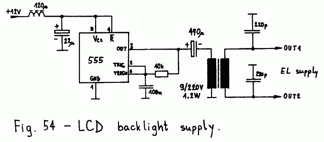
A suitable power supply is shown on Fig. 54 and includes a power oscillator (555), a step-up transformer and a few EMI filtering components. For 500Hz operation a conventional mains transformer with a laminated core can be used, either 220V/9V or 220V/6V, of course with the primary and secondary windings interchanged. A 1.2W or 1.5W transformer is usually the smallest available, although it is still quite large for this application.
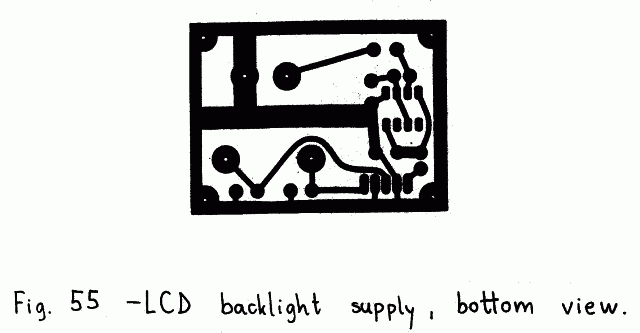
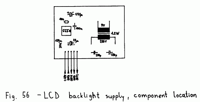
The printed-circuit board for the EL foil supply is shown on Fig. 55 and the related location of components on Fig. 56. The power drain of the whole circuit is about 50mA from a 12VDC power supply, when the output is connected to the load. Since the oscillator feedback is taken from the output (pin 3 of the 555), some 555 ICs may not operate in a stable way in this circuit. In the latter case the solution is to increase the oscillator frequency by decreasing the 100nF capacitor.
Of course, a LED backlight is much easier to use and
usually only requires a 5VDC supply.
4.14. Power supply & RESET circuit
The described GPS/GLONASS receiver is intended to be
operated from a 12V battery, with the negative grounded. This
supply voltage is common to all portable and mobile equipment.
The analog circuits of the GPS/GLONASS receiver are already
designed to operate from a +12V supply rail, since this
voltage represents a convenient choice.
Of course, digital circuits require a +5V supply voltage.
But besides the +5V supply there are other requirements.
A GPS or GLONASS receiver should include a real-time clock
that operates even when the receiver is powered down.
Similarly, the almanac data including information about the
available satellite orbits should be stored in the computer
memory when the receiver is powered down. Finally, since
the +5V power drain amounts to about one half of the total
power drain of a GPS or GLONASS receiver, the +5V supply
regulator should also have a good efficiency, especially
in a portable receiver.
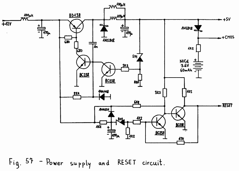
The requirements for the microcomputer power supply are therefore the same as for the DSP computer published in [1] and [2]. The original DSP computer power supply is however about 10 times too large for this application, so a scaled-down version is shown on Fig. 57. The latter includes a switching regulator from 12V to 5V, a memory (clock) backup battery and a very reliable RESET circuit.
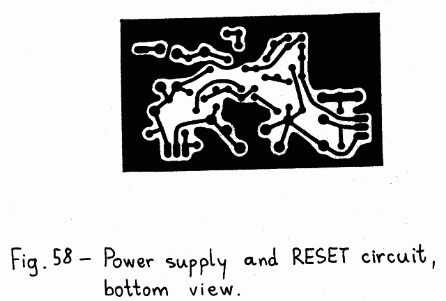
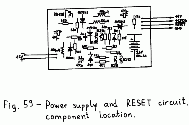
The microcomputer power supply is built on a single-sided printed circuit as shown on Fig. 58. The corresponding location of components is shown on Fig. 59. All of the resistors, diodes and chokes are installed horizontally. All of the capacitors have a 5mm pin spacing. Several mounting holes and related pads are provided for different style NiCd batteries.
The power supply is designed for a 400mA to 500mA load
on the +5V output. For this load the BD138 power switch does
not require a heatsink yet and easily available "molded"
chokes can be used in the switching regulator. In particular,
a 100uH choke with the external dimensions of a 1/2W resistor
will withstand a current of up to 200mA to 300mA, so two such
chokes are used in parallel in the switching regulator.
The total power drain when using the described power
supply and including the analog section, amounts to about 4W
for a portable GPS receiver and to about 6W for a portable
GLONASS receiver, both with the LCD backlight off.
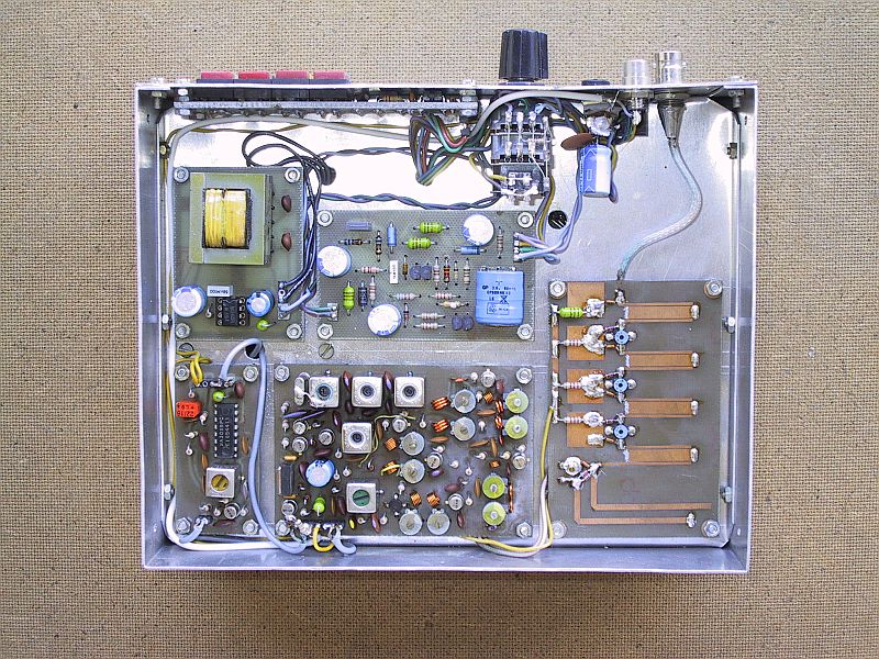
4.15. GPS/GLONASS receiver module location
A GPS or GLONASS receiver includes both low-level RF
signal amplification and processing and very noisy digital
circuits, so the module location has to be selected carefully
and some shielding is required in any case.
In the case of a GPS or GLONASS receiver operating as
a peripheral for the DSP computer, the RF part of the
receiver should be built in its own enclosure while the
dedicated DSP hardware module is plugged in the computer bus.
Of course it is assumed that the computer already has its own
shielded enclosure.
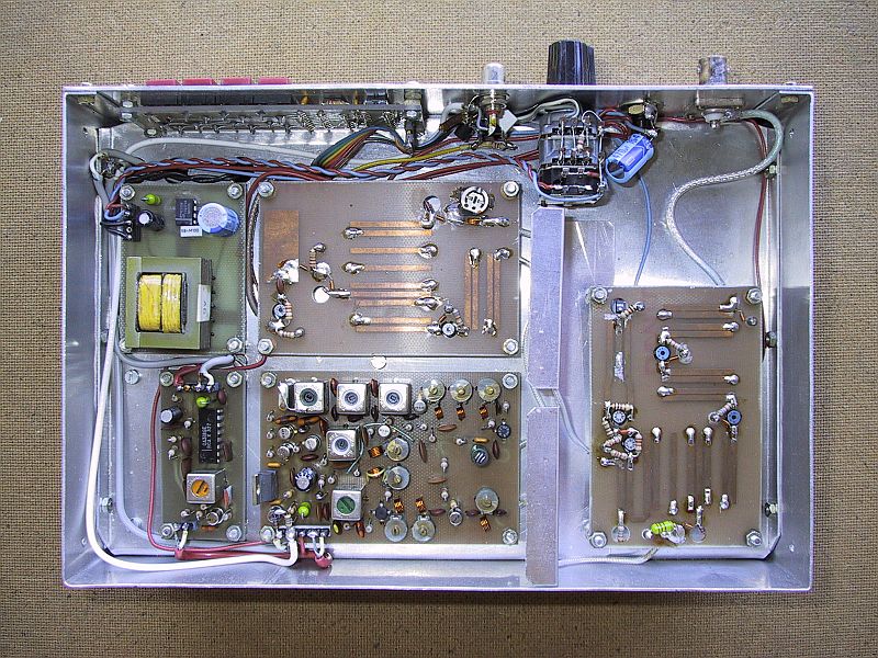
The GPS-receiver RF part needs no additional internal
shields among the three modules: RF, IF converter and IF
amplifier. The GLONASS-receiver RF part is more complicated
and requires some shielding. In particular, the GLONASS PLL
synthesizer logic needs to be well shielded from the remaining
modules: RF, IF converter, IF amplifier and PLL converter.
In the case of a stand-alone, portable GPS or GLONASS
receiver it is of course desirable to have the complete
receiver packaged in one single enclosure. It is suggested
that enclosure is made of unpainted aluminum sheet to have a
good electrical contact among the various parts. Such a
container is made of a rectangular frame and two covers
installed with self-locking screws. The frame has an
additional internal plate that divides the internal volume
in two sections shielded both from the outside and between
themselves. One of the sections is used for the noisy digital
circuits and the other for the low-level RF stages.
"Interference-neutral" modules, like the keyboard or the power
supplies may be installed in either section.
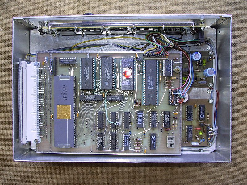
The suggested module location for a portable GPS receiver
is shown on Fig. 60. The suggested dimensions are
200mm(width)X160mm(depth)X80mm(height). The internal plate
is installed at a height of 30mm, so that the digital section
gets a volume of 200mmX160mmX50mm (top) and the analog section
gets a volume of 200mmX160mmX30mm (bottom). The internal plate
is screwed on the frame on all four sides with many screws
to ensure a good electrical shielding.
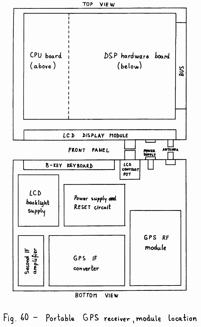
The two modules with 64-pole "eurocard" connectors are
installed on a short bus "motherboard" with just two female
connectors with the corresponding pins tied together. The bus
can be made by cutting a piece of the DSP computer bus board
or by simply installing the two connectors on a piece of an
universal board with holes in a uniform 0.1" raster.
The connections between the analog and digital parts
do not require feedthrough capacitors if they are routed
carefully, away from sensitive or very noisy components.
Sometimes it results useful to additionally ground the shields
of coaxial cables when crossing the internal plate.
The suggested module location for a portable GLONASS
receiver is shown on Fig. 61. The suggested dimensions are
240mm(width)X160mm(depth)X80mm(height). The internal plate
is installed at a height of 30mm, so that the digital section
gets a volume of 240mmX160mmX50mm (top) and the analog section
gets a volume of 240mmX160mmX30mm (bottom). Like in the GPS RX
the internal plate is screwed on the frame on all four sides.
In addition there is a small shield between the RF module
and the remaining modules in the analog part. On the other
hand, in the GLONASS receiver the computer power supply is
installed in the digital section, together with the PLL
synthesizer logic.
* * * * *