
(DESIGN)
(COSTAS)
(FRONTEND)
(SUPPLY)
(PCB)
(SHIELD)
(ASSEMBLY)
(TEST)
(HOME)
10Mbps BPSK ZIF transceivers for 1.2GHz, 2.3GHz and 3.4GHz
Matjaz Vidmar, S53MV
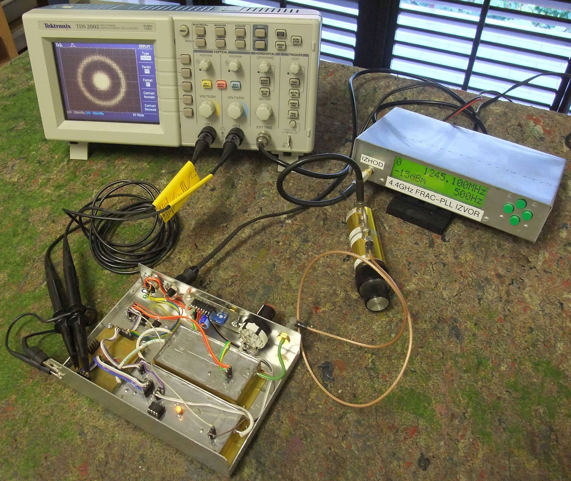
8. Testing BPSK transceivers
Testing of data transceivers may not be as straightforward as testing analog radios with a microphone and a loudspeaker. A defective data transceiver may not achieve its top performance yet providing an almost error-free link in usual conditions. Some module tests are recommended even before the assembly of the complete transceiver while other tests are performed on the complete unit.
In the described BPSK transceivers it is necessary to test the ZIF+PLL+modulator first starting with the PLL local oscillator. Check that the firmware in the PIC 12F675 matches the PLL chip ADF4351 or MAX2870. If the PLL works correctly, the lock LED should turn on a fraction of a second after applying the supply voltage.
Both the RF chips have very low LO requirements: around -20dBm for the AD8347 and around -10dBm for the AD8349. This is about 30dB less than a discrete solution with diode doubly-balanced mixers making crosstalk and shielding problems much easier. Therefore the output level of the PLL chip is intentionally set very low in the firmware. Such a low signal level may be difficult to measure with a frequency counter. A small loop probe connected to an RF spectrum analyzer may be required to check the output of the PLL synthesizer.
The Zero-IF receiving chain requires checking the gain, AGC, frequency response and quadrature of both I and Q channels. First the correct DC levels supplied by the AD8347 should be checked. All signal outputs IMXO, QMXO, I, /I, Q and Q' should be close to VREF at about 1V above ground. The AGC should be around 0.1V with no signal and may rise up to 1V by applying some input signal, all measured with a high-impedance voltmeter.
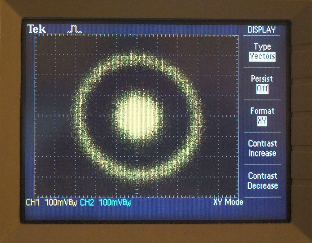
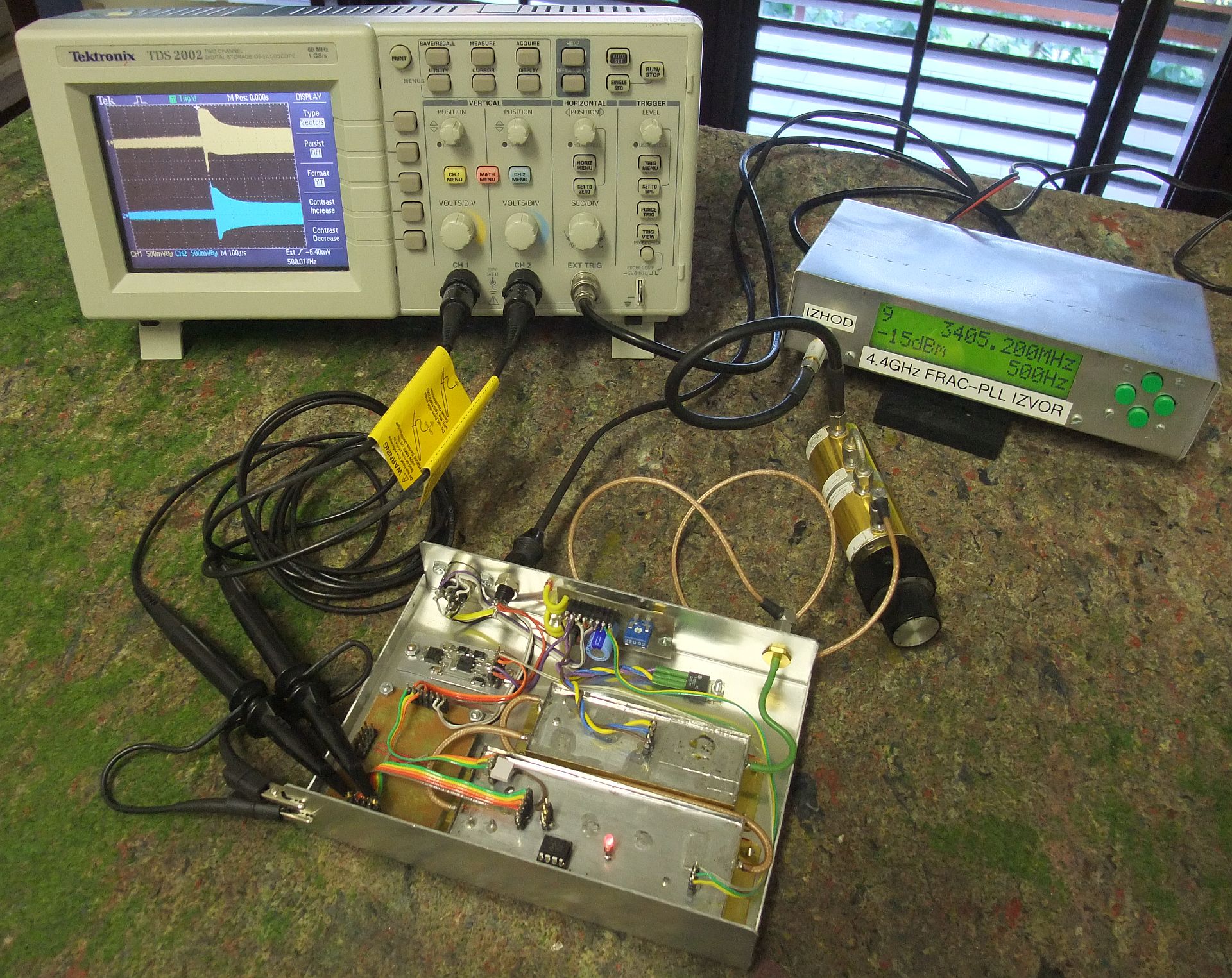
The gain, AGC, frequency response and quadrature of both I and Q channels are best tested with an RF signal generator and a dual-channel oscilloscope. The signal generator has to be set to an offset from +/-10kHz of the LO frequency up to +/-10MHz while testing a 10Mbps transceiver. For quadrature testing the RF signal generator can be unmodulated (CW). For AGC testing the RF signal generator is modulated ON/OFF with a 500Hz square wave:
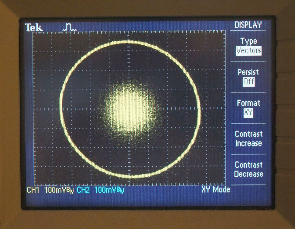
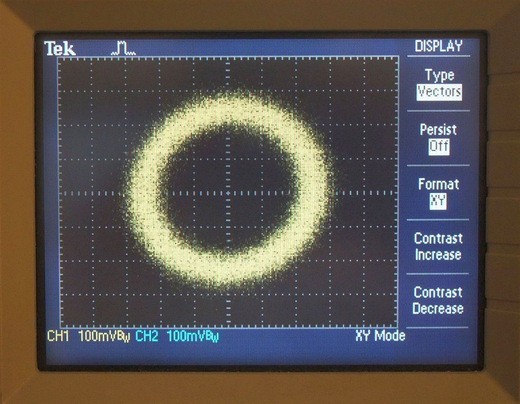
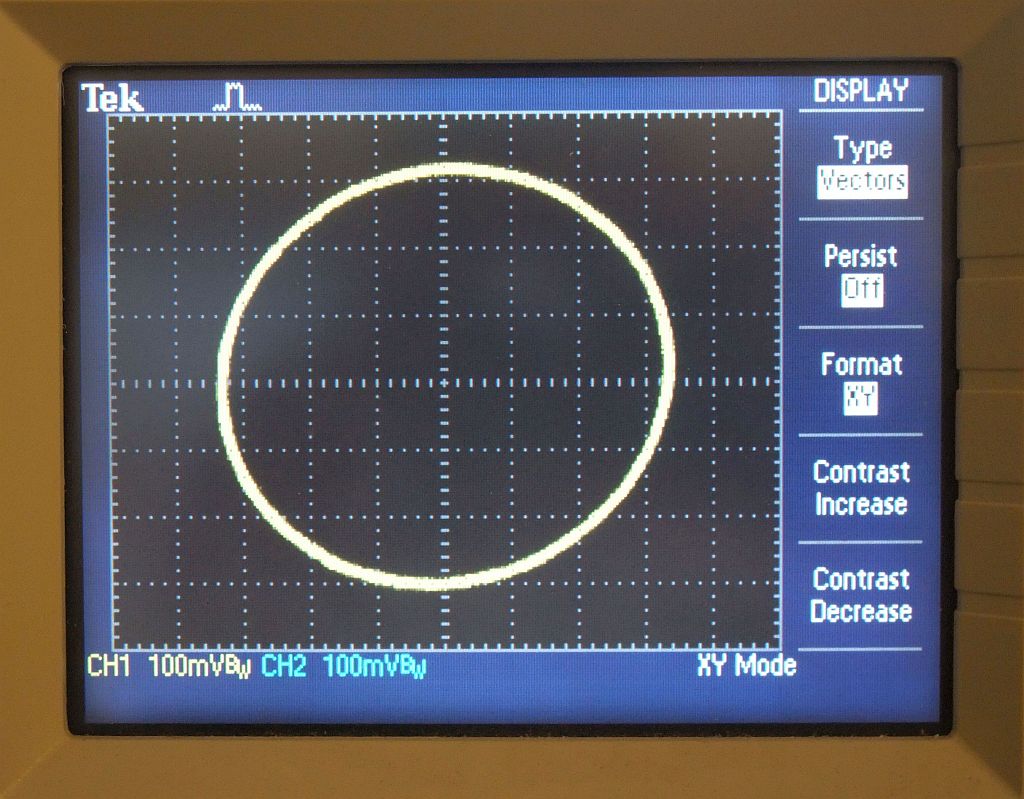
The dual-channel oscilloscope is used in the XY mode for quadrature testing. The oscilloscope should show a perfect circle. The circle degrades to an ellipse in the presence of gain and/or phase errors. A horizontal or vertical major axis signals gain errors. A 45-degree inclined ellipse signals phase errors. An ellipse axial ratio of less than 1.1 is sufficient for BPSK operation. The same "ellipse" test should be repeated for different input signal levels and different frequency offsets:

If the signal generator is modulated ON/OFF, a central noise dot will appear in quadrature testing. Nonlinear distortion will corrupt the circle into other shapes, usually towards a square.
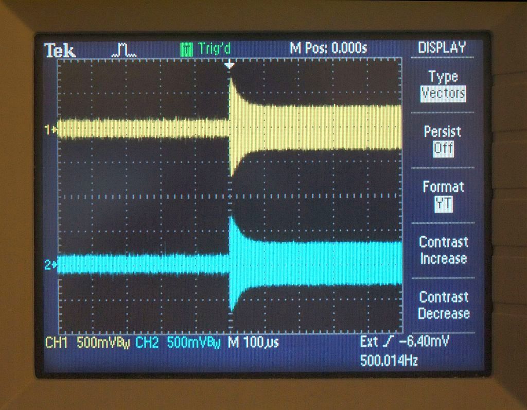
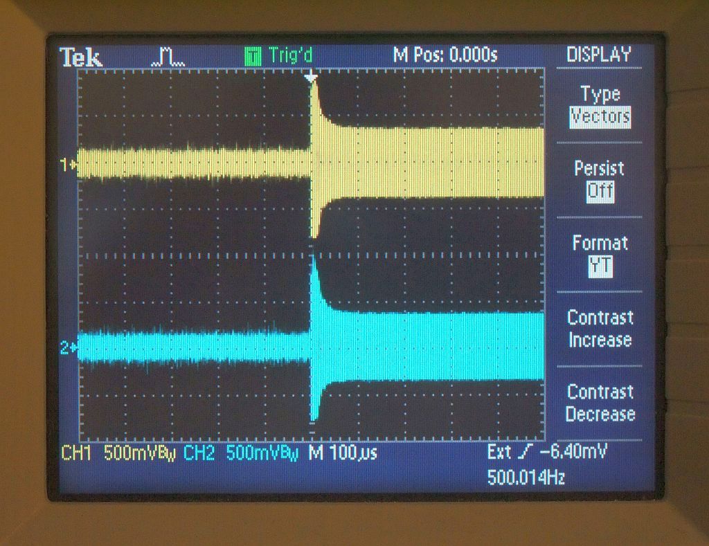
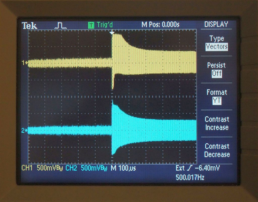
500Hz ON/OFF modulation is required for AGC testing. The oscilloscope is switched to YT mode and triggered from the modulation output of the RF signal generator. Both oscilloscope channels are used to observe the I and Q outputs simultaneously, since problems due to unwanted LO crosstalk to the RF input of the ZIF receiver may appear in only one of the I or Q outputs. The center offset is removed by AC coupling both in the ZIF receiver as well as in the oscilloscope.
The 1.25GHz BPSK receiver (perfect quadrature and AGC response) under test at 1245.1MHz -80dBm on the antenna input 500Hz ON/OFF:
AGC response of both channels at 1245.1MHz -80dBm on the antenna input 500Hz ON/OFF. The AGC-settling time is around 50 microseconds without any instabilities:
Quadrature ellipse of both channels at 1245.1MHz -80dBm on the antenna input 500Hz ON/OFF. Almost perfect circle. The central dot is noise with the source OFF:
AGC response of both channels at 1245.1MHz -50dBm on the antenna input 500Hz ON/OFF. The AGC-settling time is around 50 microseconds without any instabilities:
Quadrature ellipse of both channels at 1245.1MHz -50dBm on the antenna input on the antenna input 500Hz ON/OFF. Almost perfect circle. The central dot is noise with the source OFF:
The 3.41GHz BPSK receiver (less-than perfect quadrature and AGC response corrupted by LO crosstalk) under test at 3405.2MHz -60dBm on the antenna input 500Hz ON/OFF:
AGC response of both channels at 3405.2MHz -60dBm on the antenna input 500Hz ON/OFF. The AGC-settling time is around 100 microseconds with unsymmetrical overshoot due to the LO crosstalk:
Quadrature ellipse of both channels at 3405.2MHz -80dBm on the antenna input CW. Clean picture with the RF source always ON:
Quadrature ellipse of both channels at 3405.2MHz -50dBm on the antenna input CW. Clean picture with the RF source always ON:
What is the expected sensitivity of a BPSK receiver? There is an exact mathematical relationship between the signal-to-noise (S/N) ratio and the bit-error rate (BER) for BPSK demodulation with an ideal receiver. While the antenna noise may be very low in space communications, the antenna noise in terrestrial links is close to 290K. The sensitivity of an ideal BPSK receiver in a terrestrial link is therefore around -93.5dBm at 10Mbps and BER=1.0E-6:

A real-world receiver adds some own noise: its noise figure including the loss of the antenna switch and any antenna filters if present. A real-world BPSK demodulator may have an additional loss of about -2dB. The described BPSK receivers therefore achieve a sensitivity of around -90dBm.
The output of the BPSK modulator only provides output while driven with the required 10Mbps signal. With no modulation the power should drop to almost zero.
The Costas demodulator should be first checked unpowered. The 16-phase resistor network should present the same resistance in both I and Q diagonals and very high impedance towards ground.
After powering up the demodulator, the EPM3032ATC44 should be programmed with the BPSKX firmware through a suitable JTAG cable. A programmed and clocked EPM3032ATC44 should generate a bias voltage of around 1.25V. There should be no voltage drop (less than 1mV) on the 4.7kohm resistor jumper. If noise from the ZIF receiver is applied to the I, /I, Q and Q' inputs, the mean value of the RXM output should get close to half the supply voltage or 1.65V.
Applying a CW RF signal above -70dBm on the antenna input at an offset less than +/-100kHz (10Mbps version) or less than +/-40kHz (2Mbps version), the RXM output should switch to either the full supply voltage +3.3V or ground 0V. At larger offsets the demodulator DPLL is unable to track and the RXM output mean value stays close to half the supply voltage or 1.65V.
The RF front end should be first tested for the correct DC voltages and currents. All RF connections should be terminated to loads and/or other circuits to avoid self oscillations. These self oscillations may be strong enough to kill the PTFC270101M power LDMOS while adjusting its quiescent bias for 100mA drain current.
The noise generated by the receiving LNA should be visible (at least 20mV increase) on the AGC voltage. The 1.25GHz and 2.36GHz LNAs usually do not require any tuning. The 3.4GHz LNA requires a capacitive tuning stub (piece of tinned copper foil) to increase its gain by about +2dB and improve the noise figure.
The transmitting power amplifiers usually require little if any tuning. Improvements are usually less than +0.5dB. The transmitting power amplifier for 1.25GHz may require some tuning of the output. The transmitting power amplifiers for 2.36GHz and 3.41GHz may requires some tuning of the interstage match.
The final adjustment of the transmitter is the modulation level. The TXM input is driven either with a 10Mbps (2Mbps) pseudo-random sequence or with the output of a TNC programmed for very long synchronization headers. The nominal output power is achieved between 1/4 and 1/2 of the range of the 220ohm trimmer. Too weak modulation provides less output power. Too strong modulation provides a distorted output. The correct setting can be found with an RF spectrum analyzer. Distortion generates additional sidebands and even spectral lines at clock multiples. As a rule of thumb, the modulation trimmer is set for an output-power backoff of about -10% or -0.5dB from the maximum power.
Finally one should understand what a ZIF BPSK transceiver can do and what can theoretically not do at all. Symmetrical BPSK modulation does not maintain signal polarity. Therefore TXM data has to be differentially encoded on the transmitting end and RXM data differentially decoded on the receiving end. ZIF receivers usually do not support any DC component of the signal due to the finite LO crosstalk. Therefore TXM data has to be randomized in the transmitting scrambler and derandomized in the receiving descrambler. All these functions are provided by default in suitable TNCs, like ATNC, AATNC, EATNC, RATNC or SATNC.
(DESIGN) (COSTAS) (FRONTEND) (SUPPLY) (PCB) (SHIELD) (ASSEMBLY) (TEST) (HOME)