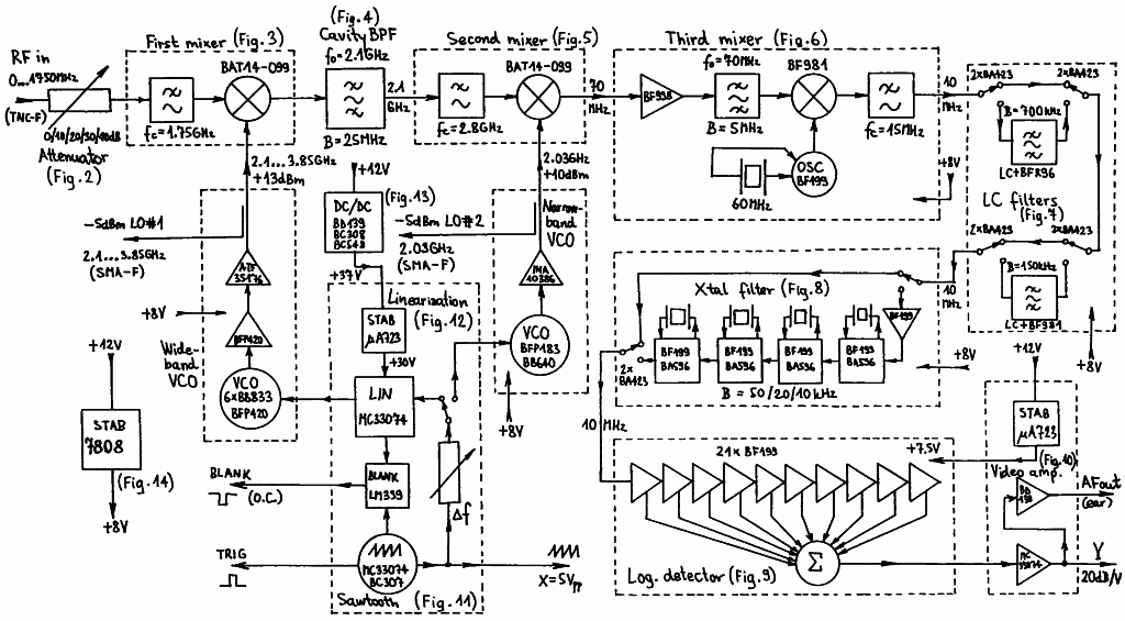
Fig.1 - Spectrum-analyzer block diagram.
(VCO)
(SA)
(TG)
(HC)
(SN)
(MC)
(LCD)
(HOME)
Spectrum Analyzer 0...1750MHz
Matjaz Vidmar, S53MV
1. Spectrum-analyzer design
Wide-band (panoramic) receivers and RF spectrum analyzers are usually designed as multiple-conversion receivers with the first IF above the maximum input-signal frequency. Amateur designs are mainly limited by the performance of the VCO used for the first frequency conversion. The 2-4GHz VCO presented in [1] and [2] allows the design of a simple spectrum analyzer covering the frequency range 0...1750MHz in a single span.
The resulting spectrum-analyzer block diagram, shown on Fig.1, was already briefly described in [1] and [2], although only the microwave VCOs were described in detail. In this article the remaining building blocks of the above-mentioned spectrum analyzer will be described in detail, as well as the overall assembly and tuning of the completed instrument.
Fig.1 - Spectrum-analyzer block diagram.
As already mentioned in [1] and [2], the described spectrum analyzer is a triple-conversion receiver with the corresponding IFs around 2.1GHz, 70MHz and 10MHz. Since both the first LO and the second LO are VCOs, the first IF may be made variable. This may be useful to shift some spurious responses of the first mixer in some difficult measurements.
The described spectrum analyzer is designed to use a standard XY oscilloscope display. Additional control signals are provided to drive different displays as well as frame memories, storage normalizers, marker generators and/or trigger frequency counters. The outputs of both VCOs are also made available to drive a tracking generator or a frequency counter. Some of these additional circuits will be described in future articles.
2. Input attenuator
The input attenuator is a simple yet important part of a spectrum analyzer. The main function of the input attenuator is reducing the signal level to avoid overdriving the first mixer. The input attenuator should therefore only include very linear components like resistors and mechanical switches.
The basic attenuator circuit is a simple "PI" or "T" resistor network. The resistor values are selected both for the desired attenuation value and input/output impedance matching. Since a "PI" or "T" network contains three independent resistors, all three quantities can be adjusted independently within certain limits: attenuation, input impedance and output impedance.
Generally speaking, attenuators can be built for any frequency provided that the resistors (and switches) are sufficiently small with respect to the wavelength and/or are designed as parts of transmission lines with carefully controlled characteristic impedances. Professional attenuators, both fixed and adjustable, are available for frequencies up to 18GHz and beyond, depending mainly on the coaxial connectors.
On the other hand, it is much more difficult to build good microwave attenuators from standard electronic components. Resistors with wire leads are only useful up to about 500MHz. SMD resistors are much better due to their smaller size and can be used up to at least 5GHz. Finding suitable mechanical switches for microwave frequencies is even more difficult.
The circuit diagram of the attenuator, shown on Fig.2, therefore can not tell much about the microwave performance of the circuit. The attenuator includes four identical "PI" networks and four DPDT switches. This design allows a nominal attenuation of 0dB to -40dB in 10dB steps.
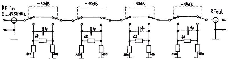
Fig.2 - Attenuator.
Standard SMD resistors of the size 0805 or smaller are certainly good enough for a 2GHz spectrum analyzer. It is much more difficult to find suitable DPDT switches with low parasitics. In the prototypes standard miniature DPDT toggle switches were used. The resulting frequency response was compensated with 1pF SMD capacitors soldered across the 68ohm resistors. Finally, the toggle switches were installed between two small printed-circuit boards to keep their impedance closer to 50ohms (to be described later in this article).
A careful construction together with some compensation capacitors allows to keep the frequency response of the attenuator within +/-1dB for frequencies up to 1GHz and within +/-2dB for frequencies up to 2GHz from the nominal attenuation value. Since the maximum power dissipation of SMD resistors is 1/8W, the maximum input power to the described attenuator is about 250mW (+24dBm). At the maximum attenuation value of -40dB this means -16dBm at the first mixer input.
Of course additional (external) high-power attenuators or couplers are required for transmitter measurements. The input attenuator of a spectrum analyzer is only intended for fine adjustments of the input signal level and/or finding the source of some signals: real signals or unwanted mixing products in the spectrum analyzer?
Finally, the described attenuator does not include any protection against DC voltages that may be present in some RF circuits!
3. First mixer
The dynamic range of any receiver depends mainly on the performance of the first mixer. The low end of the dynamic range is defined by the mixer noise figure (insertion loss) while the high end of the dynamic range is defined by the mixer distortion (intermodulation). Further, the first mixer of a spectrum analyzer may be easily destroyed by high RF levels, DC voltages and even static discharges on the input connector.
The first mixer of a spectrum analyzer should therefore both provide the best possible dynamic range and at the same time allow quick and inexpensive repair in the case of damage. The latter requirement makes commercially-available, doubly-balanced mixers with schottky quads and ferrite balancing transformers unpractical.
The described spectrum analyzer is therefore using an inexpensive double schottky diode BAT14-099 in the first mixer. The balun for the local oscillator is built from UT-085 semirigid cable, as shown on Fig.3. A completely symmetrical construction allows a balancing of at least 30dB without any tuning and more than 45dB by adding small drops of solder in the circuit. Of course the symmetry of commercially-built mixers can not be improved since the latter are built in hermetically-sealed packages.
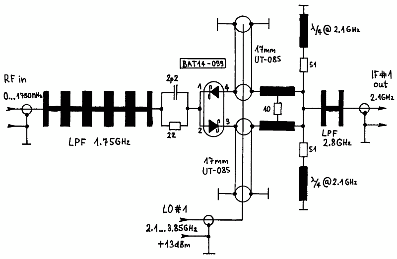
Fig.3 - First mixer.
A good mixer symmetry is required for many reasons. A balanced mixer prevents the oscillator noise from getting directly in the first IF. Further, some unwanted mixing products are suppressed in a balanced mixer. In the case of a spectrum analyzer it is especially important to suppress second-order distortion products, so that the spectrum analyzer can be used to accurately measure the suppression of the second harmonic in radio transmitters.
The first mixer module includes a microstrip low-pass filter with the cutoff frequency of about 1.75GHz. The latter should suppress unwanted responses of the spectrum analyzer in the microwave frequency range. Its insertion loss amounts to about 45dB at the first IF around 2.1GHz and becomes even higher at higher frequencies. The low-pass is followed by a RC network to slightly compensate the slow decay of the sensitivity at frequencies above 1GHz.
The mixer diode BAT14-099 is followed by several components to provide impedance matching and suppression of unwanted resonances. For example, the open end of the UT-085 balun is also used as a coupling capacitor. The two 51ohm resistors and corresponding quarter-wavelength lines provide a termination for the image frequency and other unwanted mixing products, reflected by the 2.8GHz low-pass and the following cavity bandpass filter.
4. Cavity bandpass filter
In all wide-band receivers, the first mixer should be followed by the best possible bandpass filter. In HF receivers covering 0...30MHz, a 15kHz wide crystal filter is usually used in the first IF around 45MHz or 70MHz. Considering the first IF the described spectrum analyzer at 2.1GHz, a cavity bandpass filter is the only technology that provides both high selectivity and low insertion loss.
Microwave cavities are electrically simple to describe, but usually require lots of precision mechanical work and special tools for manufacturing. Several efforts were spent in finding a reproducible cavity-filter design, made from standard materials using only simple mechanical tools.
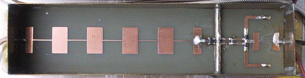
The described bandpass filter is built inside a piece of standard aluminum tube of rectangular cross-section with the external dimensions of 40mmX20mm and 2mm wall thickness. Such rectangular aluminum tube can be found elsewhere in Europe. Of course, its internal dimensions of 16mmX36mm are the most important parameter while building a cavity filter.
The construction of the cavity bandpass filter is shown on Fig.4. The filter includes five quarter-wavelength resonators made from 8mm diameter aluminum rod. All five resonators are oriented in the same direction ("comb" filter) to decrease the coupling between adjacent resonators. In this way the overall dimensions of the filter are smaller than in the case of an "interdigital" arrangement of the resonators.
Fig.4 - Cavity BPF.
The input and output couplings are made by two small rod antennas, supported by the corresponding SMA connectors. The coupling is adjusted by the length (around 27mm) of the two antennas made of thin copper tube (UT-085 shield). The coupling between resonators is defined by the distance 25mm between resonator centers and sets the filter bandwidth to about 25MHz. Five M3X20mm tuning screws are used to bring all five resonators to the desired operating frequency. The tuning screws are inserted from the opposite narrow side of the cavity and secured with a counternut after tuning.
The cross-section of the cavity is small enough that the electromagnetic field exhibits a very fast exponential decay at both ends of the rectangular aluminum tube. Covers are therefore not required for the electrical performance of the filter. On the other hand, covers are useful to keep dust and dirt outside. Covers may extend up to 10mm inside the cavity or stay at least 25mm away from the coupling antennas without having any influence on the filter performance.
The described cavity bandpass filter provides over -100dB of suppression for the second-conversion image frequency around 1.94GHz. The insertion loss is only around -2dB at the nominal first IF frequency of 2.1GHz and over -100dB outside the passband anywhere between 0 and 4GHz. Spurious higher-order resonances appear above 4GHz, when the aluminum tube starts operating as a waveguide. A cavity filter alone is therefore not sufficient. Additional microstrip low-pass filters are therefore included in both the first and second mixer modules to suppress the spurious cavity responses above 4GHz.
The described cavity design allows narrowing the passband down to just a few MHz. A bandwidth of 25MHz was selected to allow a narrow sweep of the second LO, to avoid some spurios responses of the first mixer and finally to allow for some frequency drift of the second VCO.
5. Second mixer
The requirements for the second mixer are not as far as severe as for the first mixer, since most unwanted signals have already been removed by the cavity bandpass filter. Also the signal levels are about -10dB weaker due to the conversion loss of the first mixer and cavity bandpass insertion loss. Calculations and experiments show that no amplifier stages are required between the two mixers if the maximum dynamic range is desired.
The design of the second mixer is very similar to the first mixer, except that the input and output are interchanged, as shown on Fig.5. The second mixer is also using a BAT14-099 double schottky diode and a balun made from UT-085 semirigid cable. Since the second mixer operates in a narrow frequency band, damping resistors and other compensation components are not required.
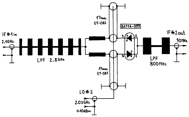
Fig.5 - Second mixer.
The second mixer module includes low-pass filters both at the input and output. The input low-pass filter cuts above 2.8GHz to suppress the spurious cavity responses above 4GHz. The output low-pass cuts above about 800MHz to suppress unwanted mixing products and feed-through of the LO signal.
6. Third mixer
The first IF of the spectrum analyzer around 2.1GHz is far too high for the different IF filters and logarithmic detector. A more suitable choice for the final IF is 10MHz. The latter can be conveniently reached from 2.1GHz in two down-conversion steps. Due to the relatively low frequencies and low signal levels, the requirements for the third mixer are not particularly severe. An additional requirement is the maximum bandwidth B=4MHz that requires a carefully designed bandpass filter at 70MHz and wide-band impedance matching at the final IF of 10MHz.
The circuit diagram of the third mixer and related components is shown on Fig.6. The circuit includes a low-noise amplifier at 70MHz, followed by a LC bandpass filter for 70MHz and a dual-gate MOSFET mixer. The 70MHz low-noise amplifier (BF998) is the only true amplifier stage in the whole receiving chain of the spectrum analyzer. The only purpose of this stage is to compensate for the conversion loss in the mixers. Any gain increase or additional amplifier stages would just impair the dynamic range of the spectrum analyzer.
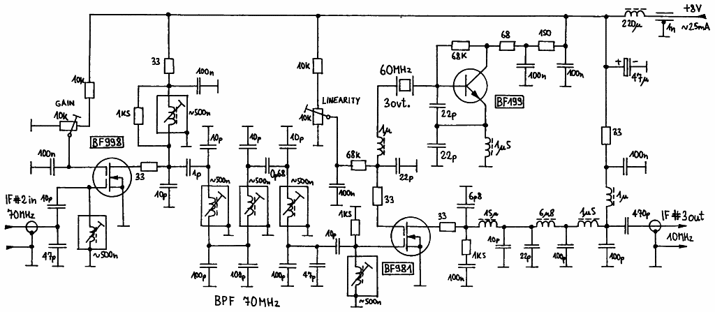
Fig.6 - Third mixer.
The LC bandpass filter at 70MHz has two functions. First, the image response of the third mixer at 50MHz has to be suppressed. Second, the widest IF bandwidth of the spectrum analyzer is defined mainly by the 70MHz bandpass filter. The bandwidth of the 70MHz LC bandpass filter itself is around 5MHz, limiting the overall bandwidth of the complete receiving chain to about 4MHz. The 70MHz LC filter is built with adjustable coils (about 500nH) wound on shielded supports for IF transformers. The input and output are terminated with 1.5kohm resistors.
The third mixer is built with a dual-gate MOSFET BF981. The input 70MHz signal is fed to the first gate while the 60MHz LO is applied to the second gate. The mixer is followed by a low-pass impedance-matching network. The latter should both remove the 60MHz LO signal and other unwanted mixing products as well as provide a wide-band transformation of the MOSFET high output impedance down to 50ohms.
The design of a suitable low-pass/matching network is complicated, since the required bandwidth is comparable to the center frequency 10MHz. Impedance matching is therefore performed in several steps with low-pass LC networks. The cicuit shown on Fig.6 allows reasonable impedance matching in the frequency band 6...15MHz and a high suppression of the 60MHz LO at the same time. The circuit is built with fixed inductors of the size and shape of 1/4W or 1/2W resistors.
The third LO includes an overtone crystal for 60MHz and a BF199 transistor. The 1.5uH inductor in the emitter of the BF199 forces the crystal to oscillate on the third overtone. The crystal is also used at the same time as a filter for the output signal fed to the mixer. The 1uH inductor in series with the crystal further reduces the amount of harmonics fed to the mixer. Finally, unwanted mixing products can be further suppressed by carefully setting the MOSFET bias with the trimmer "LINEARITY". The trimmer "GAIN" is set for the lowest practical gain of the BF998 that does not impair the noise figure of the whole spectrum analyzer.
7. LC filters
The output of the third mixer can be fed directly to the input of the logarithmic detector, setting the IF bandwidth to about 4MHz. If a narrower IF bandwidth is desired, additional bandpass filters are required between the third mixer and the logarithmic detector. LC filters can be used for bandwidths above 100kHz, while crystal filters are required for even narrower bandwidths.
A spectrum analyzer should include several different IF filters, to be included as required in the IF chain. Filter switching can hardly be performed by standard mechanical switches only, since a crosstalk better than -100dB is required between the input and output of a filter. A better solution is electronic filter switching with PIN diodes. Each filter should also include an amplifier to compensate for the insertion loss of the filter. In this way the measured signal strength will remain the same while switching among different IF filters.
Professional spectrum analyzers usually allow the selection of the IF bandwidth in steps of 1/3/10 etc. On the other hand, practical requirements show that just a few different bandwidths are required above 100kHz. Many different bandwidths are only required below 100kHz, where the IF bandwidth also defines the sweep time and limits the display update frequency.
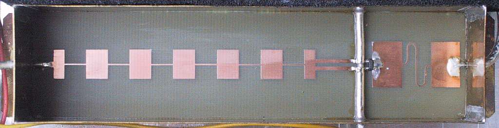
The described spectrum analyzer includes two different LC filters with the bandwidths set to 700kHz and 150kHz. In addition, the crystal filter bandwidth can be adjusted in smaller steps to 50kHz, 20kHz or 10kHz. Finally, with no additional filters an IF bandwidth of 4MHz is obtained, providing a total selection of six possible IF bandwidths.
The two additional LC filters are shown on Fig.7. Each filter includes a switching network with four diodes BA423. The filter is inserted in the IF chain by simply applying the corresponding +8V supply. At the same time the BF199 transistor cuts the direct signal path and further improves the crosstalk attenuation between the input and output of the filter.
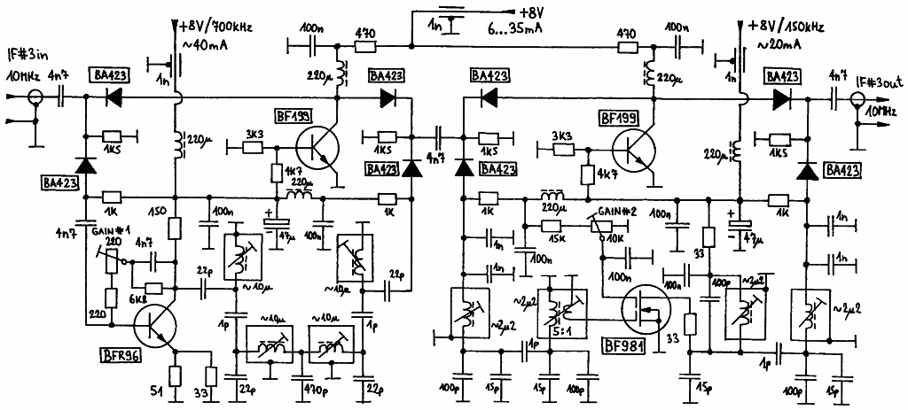
Fig.7 - LC filters.
The 700kHz wide LC filter includes four adjustable coils (about 10uH), wound on shielded supports for IF transformers. The BFR96 amplifier compensates the insertion loss of this filter. Of course the exact amount of gain depends on the loss in the coils and can be adjusted with the 220ohm trimmer.
The 150kHz wide LC filter includes two separate filters, each including two tuned circuits. The required inductances are in the range of 2.2uH. All four coils are wound on slightly larger shielded supports for IF transformers to achieve an unloaded Q of about 100. The insertion loss of both narrow LC filters is compensated by the BF981 amplifier. The gain of the latter is adjusted by the bias voltage (10kohm trimmer) on the second gate.
The LC filter module requires three different supply voltages. The +8V supply should be present at all times to bypass the filters while the latter are turned off. The +8V/700kHz supply inserts the 700kHz wide filter while the +8V/150kHz supply inserts the 150kHz wide filter. Both the input and output of the module should remain matched to an impedance of 50ohms at all times.
8. Crystal filter
Spectrum analyzers require somewhat different IF filters than those installed in communication receivers. Communication receivers usually require filters with a flat passband, to avoid modulation distortion, and a very steep increase of the insertion loss immediately outside the useful passband, to reject adjacent channels. Such filters are not suitable for spectrum analyzers, since their time response is rather slow (ringing!) compared to the filter bandwidth.
A slow filter response and/or ringing is especially harmful at small bandwidths, where the time response of the filter defines the sweep time and display update period. Commercial crystal and ceramic filters are therefore almost useless in spectrum analyzers. A suitable crystal filter or set of different filters has to be specially built for a spectrum analyzer.
A spectrum-analyzer IF filter should have a "triangular" frequency response with a sharp peak and smoothly and symmetrically increasing attenuation outside the passband. In practice this requires under-critically-coupled resonators or better a series connection of several single-resonator filters and buffer amplifiers, to avoid any interaction among the resonators.
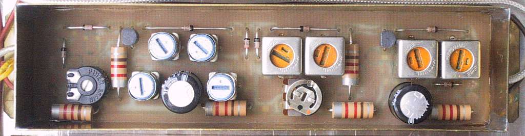
The crystal filter shown on Fig.8 includes a series connection of four independent, single resonator filters. BF199 emitter followers are used to avoid unwanted coupling among the crystals. Each individual filter includes a single crystal in a balanced network. The capacitive trimmer is used to compensate the capacitance of the crystal. The 10uH center-tap coil resonates with the 68pF capacitor and compensates the remaining parasitic capacitances of the circuit.
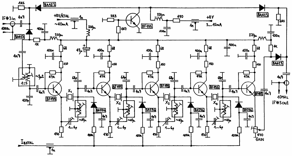
Fig.8 - Crystal filter.
The bandwidth of a single-crystal filter depends mainly on the source and load impedances. The source impedance is kept low by the previous emitter follower. The load impedance is adjustable, since a PIN diode BA596 is connected in parallel to the input of the following emitter follower. The filter bandwidth is therefore adjustable with the DC current IBXTAL fed to the four BA596 PIN diodes.
The crystal filter module includes a switch with four diodes BA423 to insert the filter in the IF chain. The supply voltage +8V should be present at all times to bypass the crystal filter while the latter is turned off. The supply voltage +8V/XTAL inserts the crystal filter. The insertion loss of the latter is mainly compensated by the emitter followers. Some additional gain is provided by the 1:5 step-up transformer at the input, followed by the first emitter follower. The overall gain is adjusted by the 470ohm trimmer on the output.
9. Logarithmic detector and video amplifier
A spectrum analyzer differs from a communication receiver also in the type of detector used. Spectrum analyzers use a logarithmic amplitude display with a very wide span of 80...100dB while communication receivers use linear detectors. A spectrum-analyzer display is therefore more similar to the operation of the S-meter of a communication receiver.
Some inexpensive commercial spectrum analyzers (Hameg) and many amateur designs in fact use the S-meter output of popular FM-demodulator chips as a logarithmic detector. This is a very poor technical solution, since the S-meter output of most FM-demodulator chips is very inaccurate and has wide deviations from the ideal logarithmic curve. Further, the dynamic range of most single-chip logarithmic detectors hardly exceeds 70dB. Chips with a wider dynamic range require interstage bandpass filters to limit the wide-band noise.
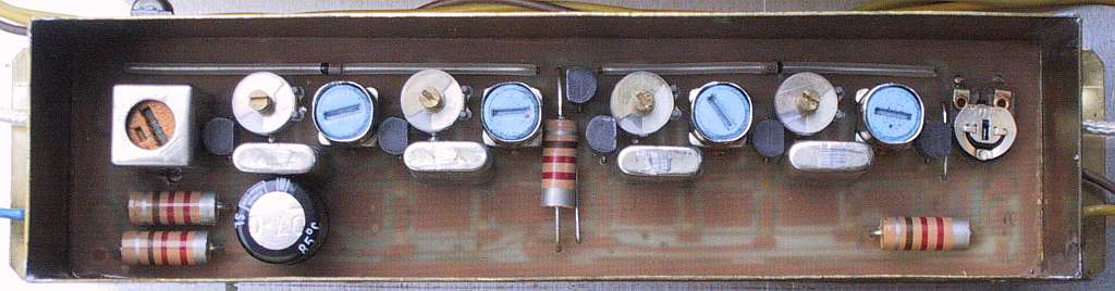
A logarithmic detector for a serious instrument therefore has to be built from discrete transistors, resistors and capacitors as shown on Fig.9. The circuit includes a series connection of ten identical stages, operating as limiting amplifiers and as linear detectors at the same time. Each stage includes a balanced amplifier, allowing a very high overall gain without instabilities and a precisely-defined saturation mechanism. The logarithmic response is obtained as a sum of linear responses that saturate above a certain level, provided that the gain of each single stage does not exceed 10...12dB.
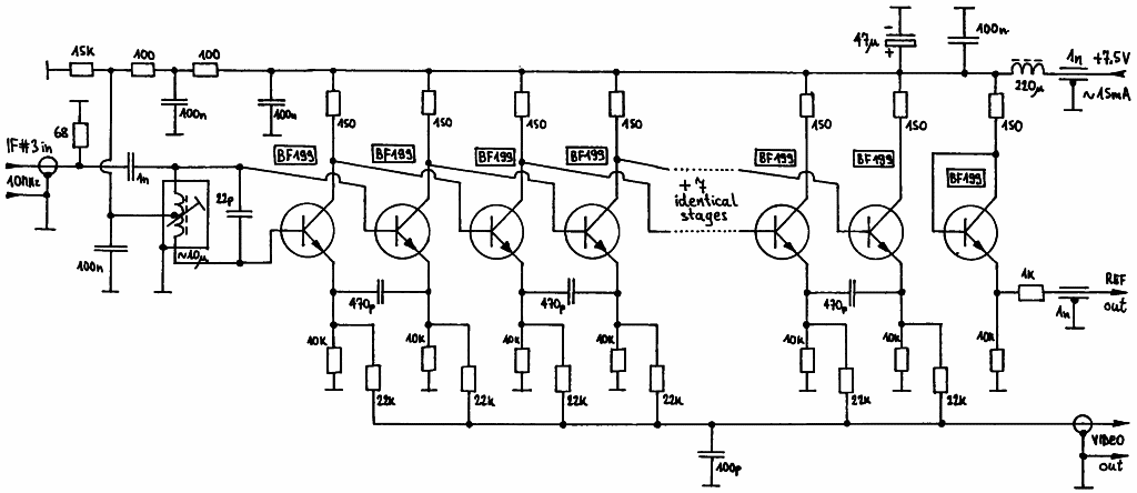
Fig.9 - Logarithmic detector.
Similar balanced amplifier chains are used as FM limiters in all known integrated circuits. The main difference between the FM chips and the discrete circuit on Fig.9 are the 470pF emitter-coupling capacitors. The latter can not be built inside a monolithic integrated circuit. The emitter-coupling capacitors allow a simple setting of the bias point and center frequency of the logarithmic detector.
Since the described logarithmic detector does not amplify DC or very low frequencies, "1/f" noise can be avoided resulting in an up to 20dB increase of the dynamic range. The noise level of the described detector is around -105dBm, while the logarithmic response is acceptable up to -10dBm, resulting in a dynamic range of at least 95dB. Another advantage of the described circuit is that the output does not saturate but becomes linear for an additional increase of the input signal level of 10...15dB beyond the nominal logarithmic response. The latter is very useful to clearly indicate excessive signal levels on a spectrum-analyzer display.
A drawback of the described circuit is a rather low output voltage, only around 100mV difference for a dynamic range of almost 100dB. The output video signal is therefore related to a reference voltage provided by a dummy BF199 amplifier, operated at the same current as the remaining twenty BF199s used in real amplifier stages. Without this compensation the output voltage would change by 2mV (meaning 2dB!) for each degree of temperature change.
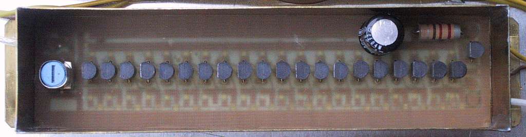
The described logarithmic detector requires a video amplifier to boost the output signal level. A suitable circuit is shown on Fig.10. The overall voltage gain amounts to about 50 and is distributed among three operational amplifiers to improve the video bandwidth. The fourth operational amplifier from the MC33074 boosts the reference. The MC33074 includes four relatively fast operational amplifiers (unity-gain bandwidth 4MHz), so that the bandwidth of the overall video amplifier is about 500kHz.
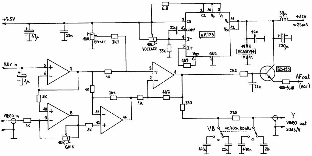
Fig.10 - Video amplifier.
The video amplifier includes two trimmers to adjust the offset (DC component) and gain. The gain should be set for an output of 20dB/V. The output circuit includes a simple video low-pass filter to limit the video bandwidth to 20kHz or 1kHz. An additional audio output is provided to drive earphones with the emitter follower BD139. The video amplifier module also includes a uA723 regulator to supply the logarithmic detector.
10. Sawtooth generator and linearization
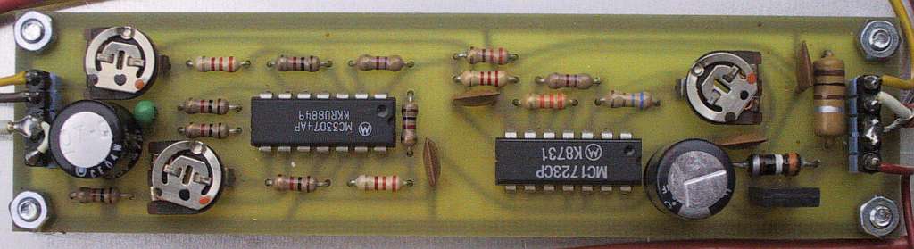
Almost any oscilloscope can be used as a display for the described spectrum analyzer. Although most oscilloscopes have built-in a sawtooth generator for the horizontal deflection, the generated sawtooth is usually an internal signal inside the oscilloscope and is not made available externally. A spectrum analyzer should therefore include its own sawtooth generator to drive the oscilloscope in the XY mode or synchronize the internal sawtooth generator in the oscilloscope.
The spectrum-analyzer sawtooth generator is shown on Fig.11. The shortest sweep time is set to about 20ms or in other words corresponding to a 2ms/div sweep on the oscilloscope. The sweep time can be increased up to 20 times with the 220klog potentiometer. On the other hand, sweep times shorter than 20ms usually make no sense in a RF spectrum analyzer.
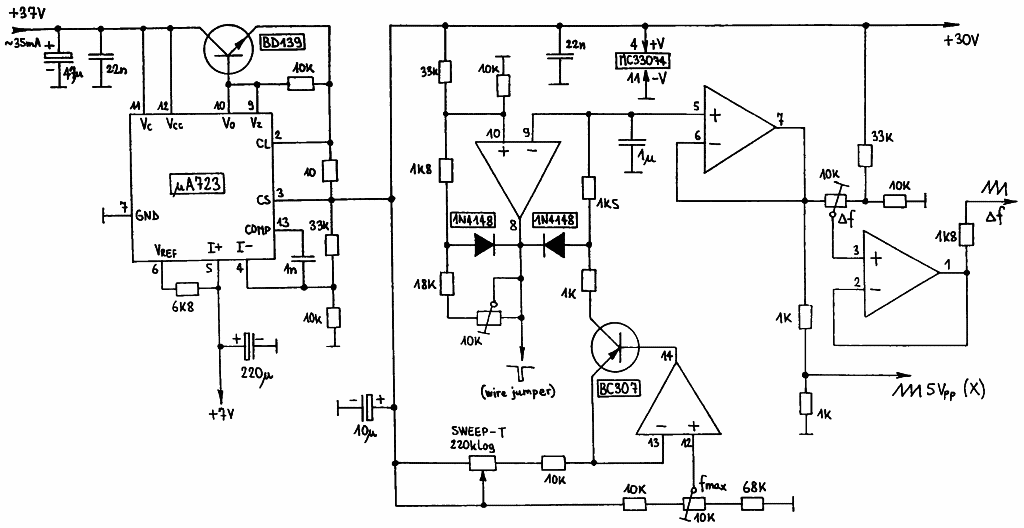
Fig.11 - Sawtooth generator.
The sawtooth generator is built with a quad operational amplifier MC33074. The MC33074 performs different functions: constant-current source, sawtooth oscillator and two output amplifiers. The circuit provides two sawtooth signals for the VCO sweep and display sweep as well as trigger pulses. The supply voltage is stabilized to 30V with the integrated regulator uA723 and BD139 power transistor.
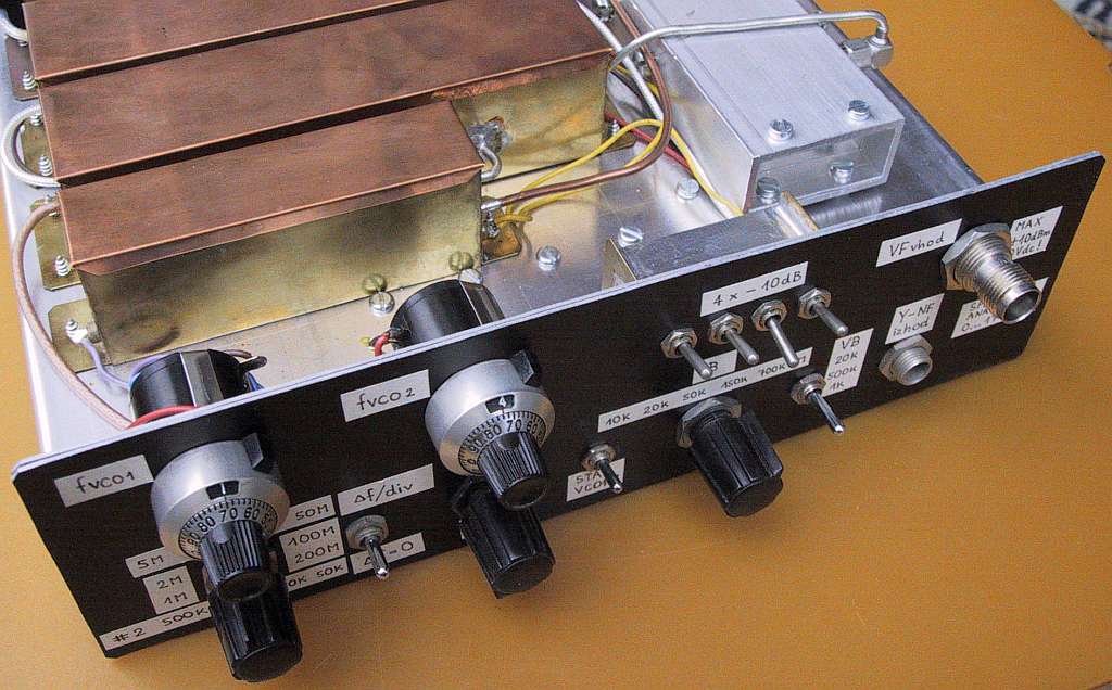
The sawtooth signal may sweep the first VCO (wide scans), the second VCO (narrow scans) or none of them in the zero-span mode. The sawtooth amplitude defines the span width. Besides the span width also the center frequencies of both VCOs have to be set to the desired values.
The described functions require several switches, selectors and potentiometers on the front panel of the spectrum analyzer. Their wiring is shown on Fig.12 together with the linearization circuit for the wide-band VCO. The center frequencies of both VCOs are set with 10-turn Helipots. The span width is set with a selector in steps 1/2/5/10 etc. At 500kHz/div and narrower spans the second VCO is swept, while the frequency of the first VCO can be additionally stabilized with the STAB VCO#1 switch. Finally, the zero-span function is activated by yet another switch that removes the sawtooth and connects 47uF capacitors in parallel with the control inputs of both VCOs.
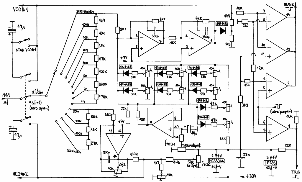
Fig.12 - Linearization.
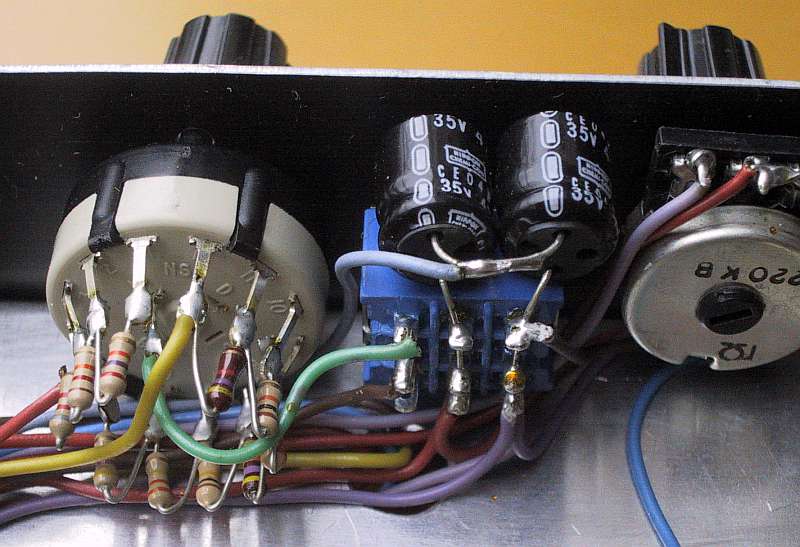
As already described in [1] and [2], the frequency response of the wide-band VCO with six BB833 varactors is quite nonlinear. The tuning slope is the steepest around the center frequency of the VCO coverage, where the tuning slope reaches 120MHz/V at a tuning voltage around 7V. At lower voltages the tuning slope decays slowly to about 90MHz/V on the lower end. The tuning slope is much more nonlinear in the upper part, where the tuning slope may decay below 10MHz/V at the maximum frequency.
The linearizer circuit includes two operational amplifiers. A negative feedback defines the minimum gain at an output voltage of about 7V. At lower or higher output voltages some positive feedback is switched in through resistive dividers and diodes. The positive feedback increases the gain of the amplifier to compensate for the decay of the tuning slope of the wide-band VCO.
A linearization of the narrow-band VCO is not required, since the latter is only swept over a small fraction of its frequency coverage. A single operational amplifier is required to drive the narrow-band VCO, since the polarity of the sawtooth has to be inverted considering the frequency conversions used in the spectrum analyzer. For the same reason it makes sense to interchange the connections to the Helipot that sets the center frequency of the narrow-band VCO (+30V on the beginning and ground on the end of the Helipot scale).
The blanking generator includes a quad voltage comparator LM339. Two comparators are used just as amplifiers for the trigger pulses to enable blanking during retrace. The other two comparators check the control voltage of the wide-band VCO, turning the display off when the VCO is tuned out of range. The LM339 comparators have open-collector outputs and the final blanking signal is obtained from a wired-or connection of three LM339 outputs.
The linearizer (another MC33074) and blanking (LM339) circuits receive the same +30V supply as the sawtooth generator. The +7V reference voltage is obtained directly from the uA723 regulator on the same printed-circuit board.
11. Power supply
The described spectrum analyzer is designed for a nominal DC supply voltage of 12VDC, negative grounded, with reasonable tolerances (10...15V). Of course, internally the spectrum analyzer requires many different supply voltages. There are also differences in the stability requirements. Some modules require very stable and well-filtered supply voltages while others are more tolerant.
Varactor diodes inside both VCOs require very stable voltages up to about +30V. Therefore the corresponding drivers require a very stable +30V supply. Considering the voltage drop in the uA723 regulator and BD139, a DC/DC converter with an output voltage of about +37V is required, as shown on Fig.13. The DC/DC converter includes a power oscillator with the transistors BC308 and BD139. Voltage spikes from the 100uH inductor are rectified by the 1N4148 diode to charge the 47uF electrolytic capacitor. When the voltage on the latter exceeds +37V, the two 18V zener diodes turn on the BC548 to stop the oscillator.
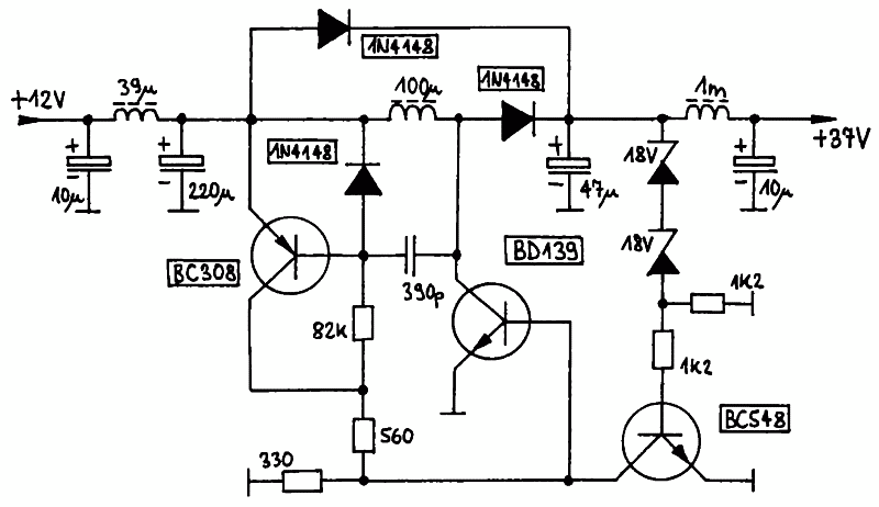
Fig.13 - DC/DC converter.
Of course, a DC/DC converter is a potential noise source to be built inside a sensitive piece of test equipment. Both input and output of the DC/DC converter are well filtered with the 39uH and 1mH chokes as well as several electrolytic capacitors. The DC/DC converter is further built on its own printed-circuit board to be installed far away from the more sensitive circuits of the spectrum analyzer.
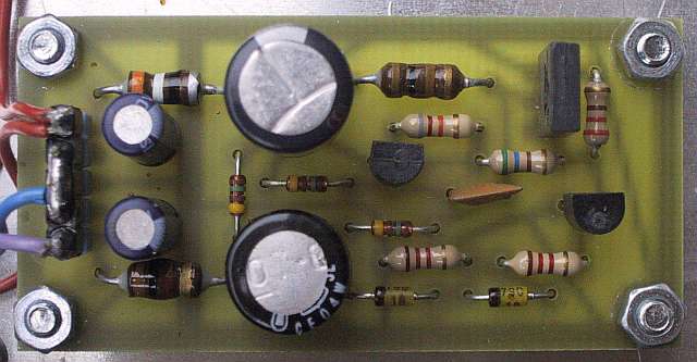
The power supply of the remaining circuits of the spectrum analyzer is shown on Fig.14. The input voltage +12V is first filtered with the VK200 choke and then fed to the DC/DC converter, to the video amplifier and to the 7808 regulator. The latter provides a stabilized +8V supply for most circuits of the spectrum analyzer. The 7808 regulator uses the baseplate of the spectrum analyzer as a heatsink and is installed together with the VK200, 470uF electrolytic capacitors and protection diode close to the +12V supply connector.
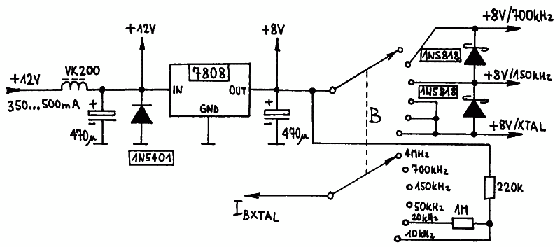
Fig.14 - Power supply.
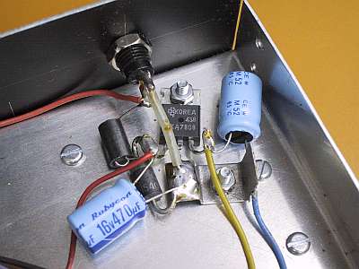
Fig.14 also shows the IF-bandwidth switching. The latter requires a two-section, six-way selector. One section of the selector is used to switch the +8V supply voltage to different filters. The two 1N5818 schottky diodes keep previous filters inserted while new filters are added in the IF chain. The second section of the selector sets the current in the PIN diodes that define the bandwidth of the crystal filter.
12. Construction tips
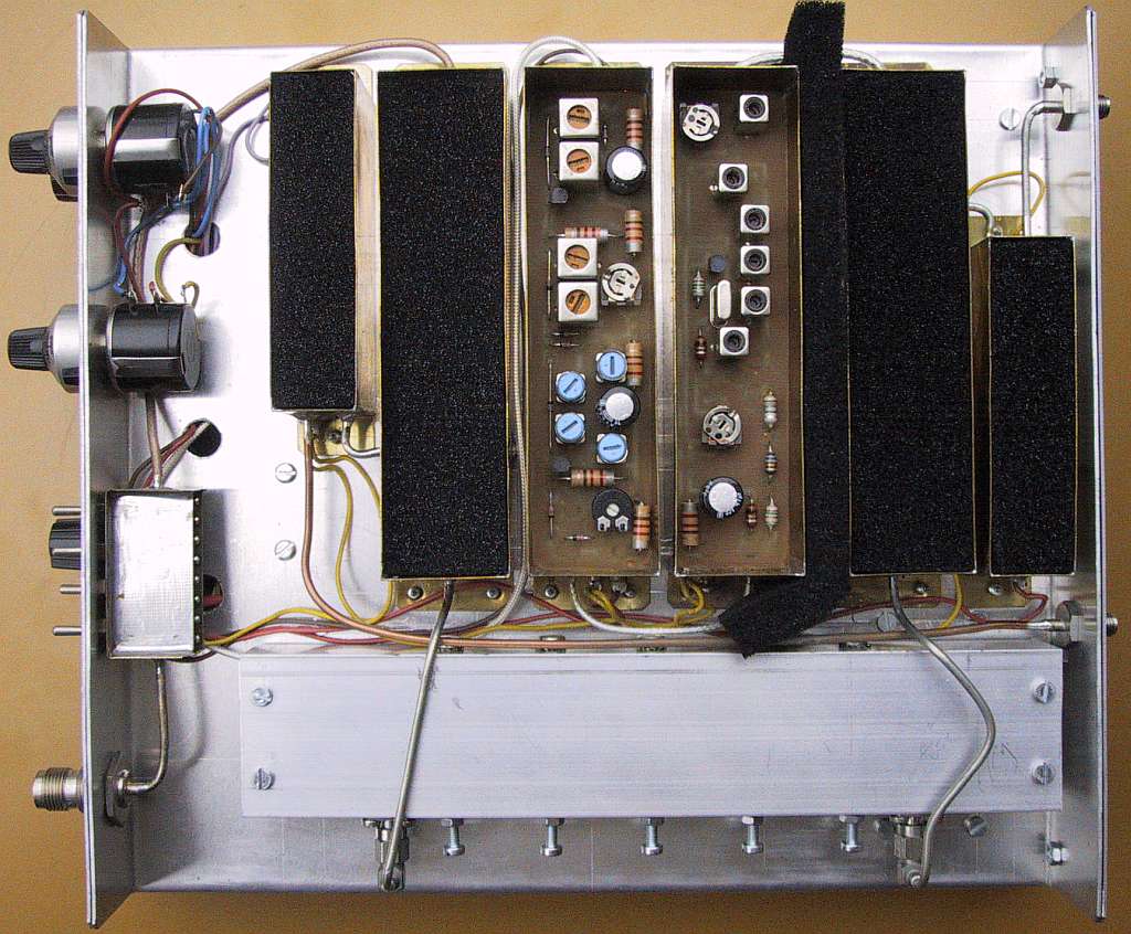
A spectrum analyzer is a sensitive receiver operating over a wide frequency range. The circuits of a spectrum analyzer therefore require considerably more and better shielding when compared to conventional communication equipment. Better shielding also requires a larger number of shielded modules that contain just a few electronic components each. Besides shielding, microwave absorbers are required outside and inside some shielded enclosures.
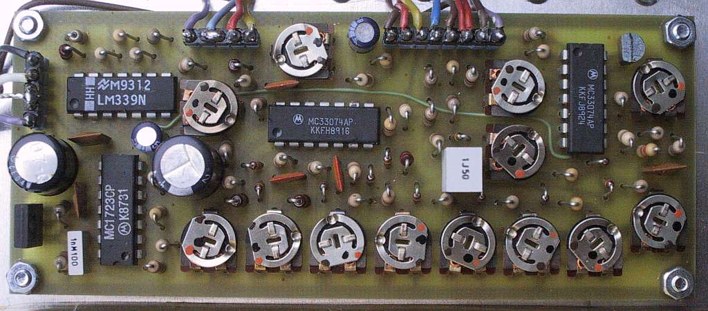
The spectrum-analyzer modules can be roughly divided in three groups: (1) microwave modules built as microstrip circuits inside shielded boxes, (2) IF modules built on single-sided printed-circuit boards inside shielded boxes and (3) video/supply modules that do not require special shielding.
The microstrip printed-circuit boards (except the VCOs published in [1] and [2]) are shown on Fig.15. All microstrip circuits are etched on double-sided, 0.8mm-thick FR4 laminate. Only the upper side is shown on Fig.15, since the bottom side is not etched to act as a groundplane.
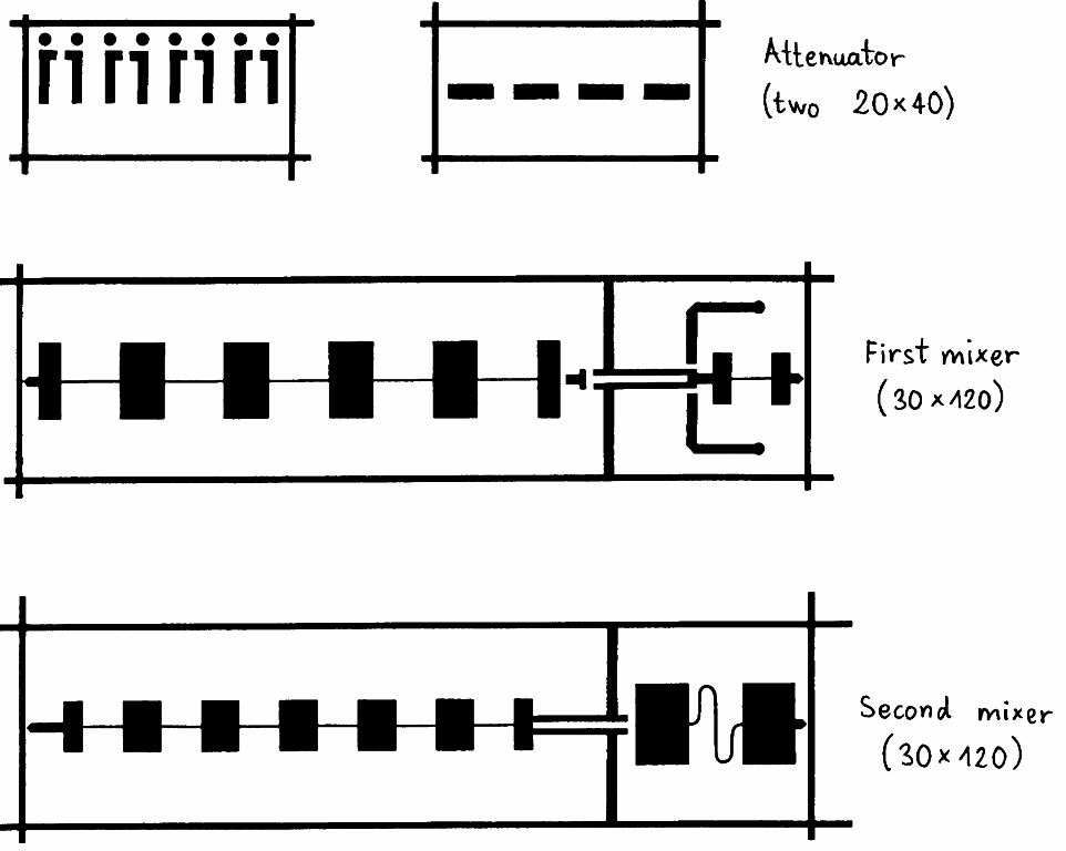
Fig.15 - Microstrip circuit boards (150dpi).
Only SMD components of the size 0805 or smaller should be installed on the microstrip circuit boards. The SMD components are grounded through 2.5mm diameter holes, covered with 0.1mm-thick copper foil on the groundplane side and filled with solder before installing the SMD components. The completed microstrip boards are soldered in brass frames and covered with a shielding cover. A piece of 1cm-thick microwave absorber foam should be installed under the whole surface of the shielding cover to suppress parasitic resonances of the shielding enclosure.
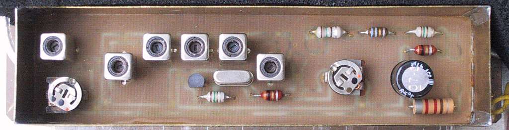
The IF printed-circuit boards, shown on Fig.16, are all etched on single-sided, 0.8mm-thick FR4 laminate. SMD components should be soldered first: resistors, capacitors and semiconductors. The printed-circuit boards are designed for SMD-component sizes 0805 or 1206. Inductors, IF transformers, trimmers, BF199 transistors, BA423 diodes, crystals and electrolytic capacitors are installed as conventional "through-hole" components from the other side.
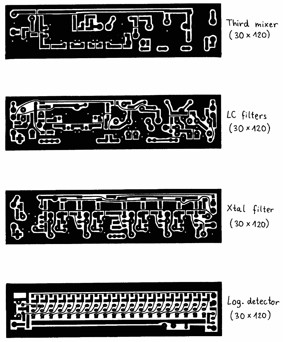
Fig.16 - IF circuit boards (150dpi).
The IF printed-circuit boards are also soldered in brass frames just like the microstrip boards. Of course, the IF modules do not require any microwave absorber foam under the cover nor any special shielding on the bottom. The supply voltages go through feed-through capacitors soldered in the narrow sides of the brass frames while the IF cable shields are soldered directly to the brass frames.
The video/supply printed-circuit boards, shown on Fig.17, are all etched on single-sided, 1.6mm-thick FR4 laminate. All of the components are conventional types with wire leads for "through-hole" installation. The resistors and diodes are installed vertically on the sawtooth and linearization module to save some space. The video/supply modules do not require any shielding and are installed on the baseplate with four M3 screws in the corners. All connections go through simple connectors made from quality IC sockets.
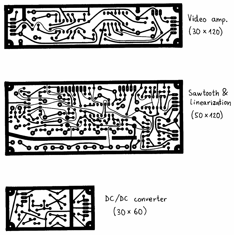
Fig.17 - Video/supply circuit boards (150dpi).
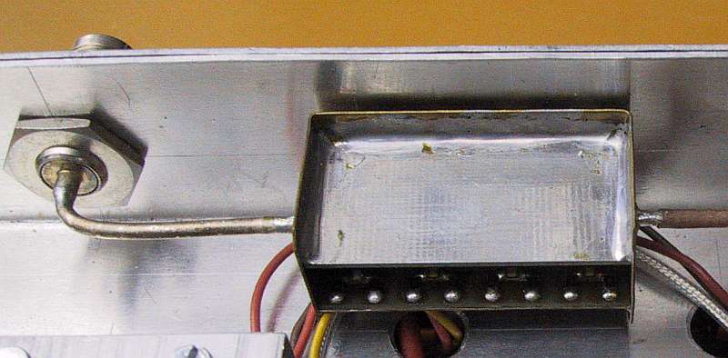
The shielded enclosures of the RF/IF modules are shown on Fig.18. The input attenuator includes four miniature DPDT toggle switches installed in a sandwich between two microstrip boards. The microstrip boards are soldered to an "U"-shaped piece of 0.5mm-thick brass sheet. The four toggle switches are installed in 5mm diameter holes, while two 3.2mm diameter holes are provided for the input and output coaxial cable. The input attenuator does not require a shielding cover.
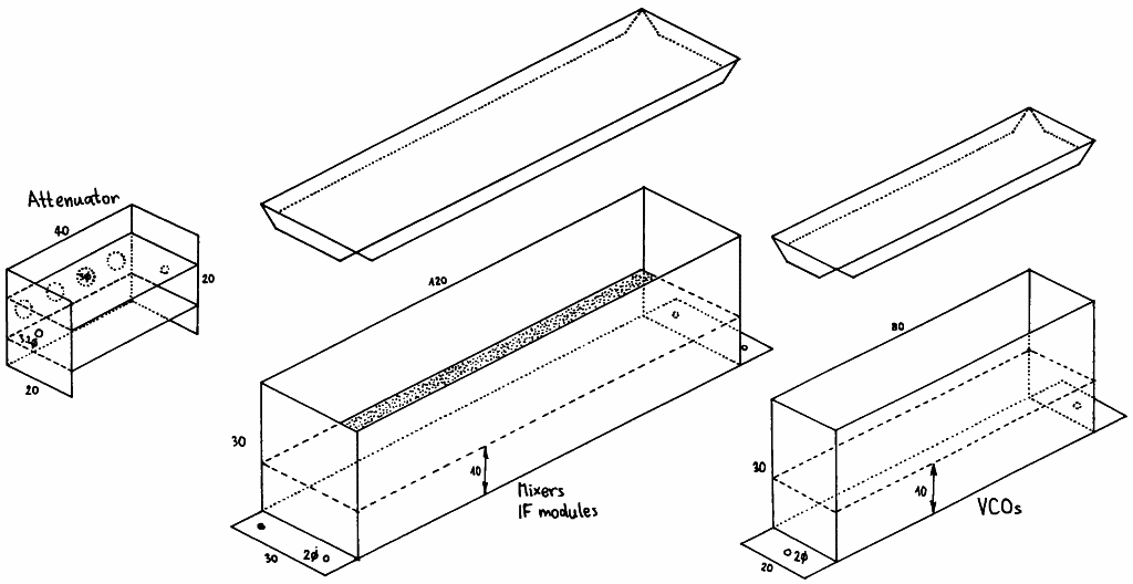
Fig.18 - Shielding of RF/IF modules.
Both microwave mixers and all four IF modules are installed in a brass frame with the dimensions 120mmX30mm, while the two VCOs are installed in similar frames with the dimensions 80mmX20mm. All frames are made from 0.5mm-thick brass sheet. Covers are also made from brass, although somewhat thinner brass sheet (0.4mm or even 0.3mm) is sufficient.
Both microwave mixers include baluns made from UT-085 semirigid cable. The shield of the latter is first tinned for a length of about 35mm to let expand the teflon dielectric. Then the shield is cut 17mm from the open end and pulled away to obtain a 1mm-wide gap. Such a prepared cable end is then soldered on the microstrip circuit board and the board is then soldered in the brass frame. The balun cable pops out of the frame for about 2mm on one side, while a longer cable (20-25mm) is available on the other side to connect the VCO.
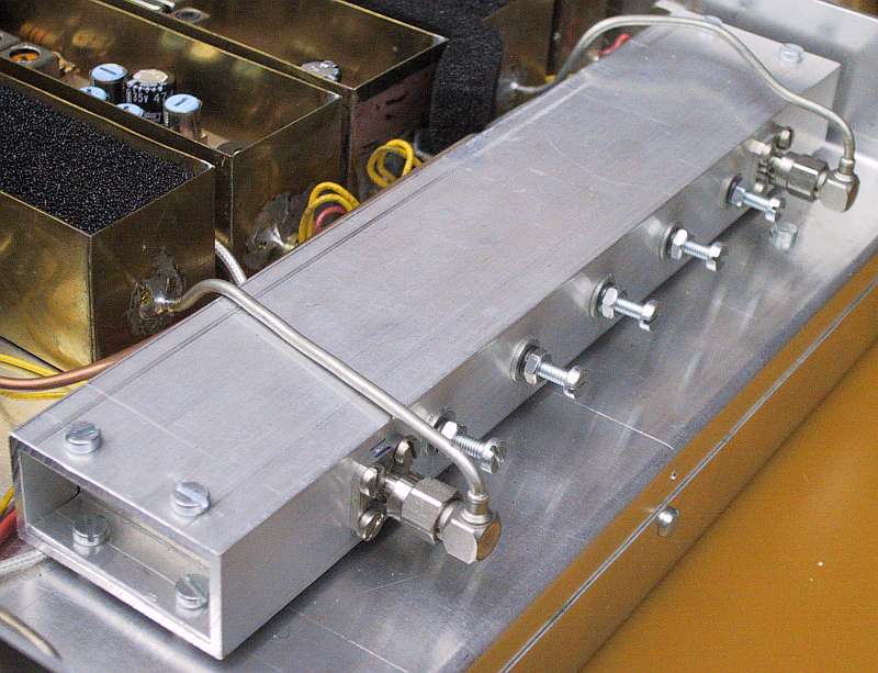
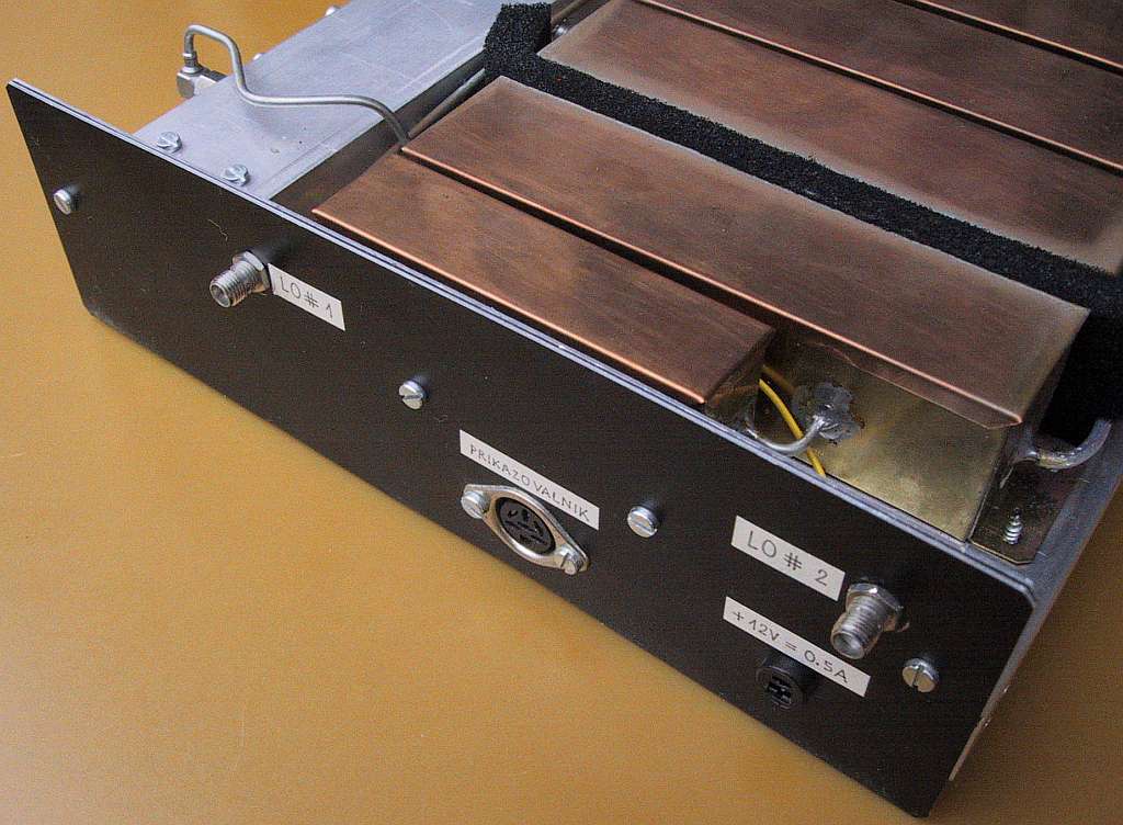
The overall spectrum-analyzer module location is shown on Fig.19 inside an aluminum box with the following dimensions: width 220mm, depth 240mm and height 65mm. A central baseplate (1mm-thick aluminum) holds all of the modules and divides the useful volume in two sections, each 32mm high. The top section may require a piece of microwave absorber between the second and third mixers.
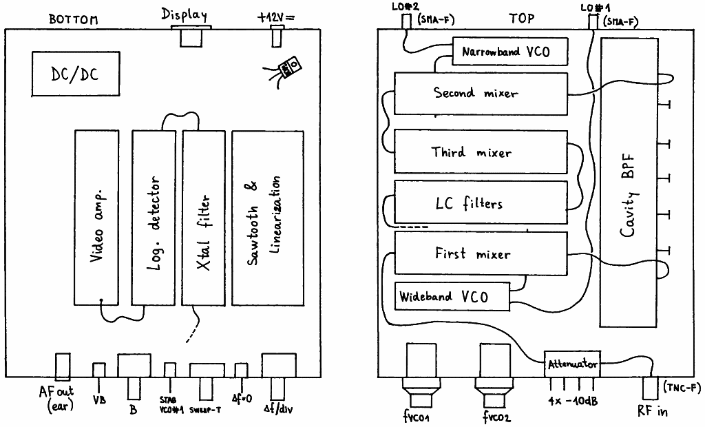
Fig.19 - Spectrum-analyzer module location.
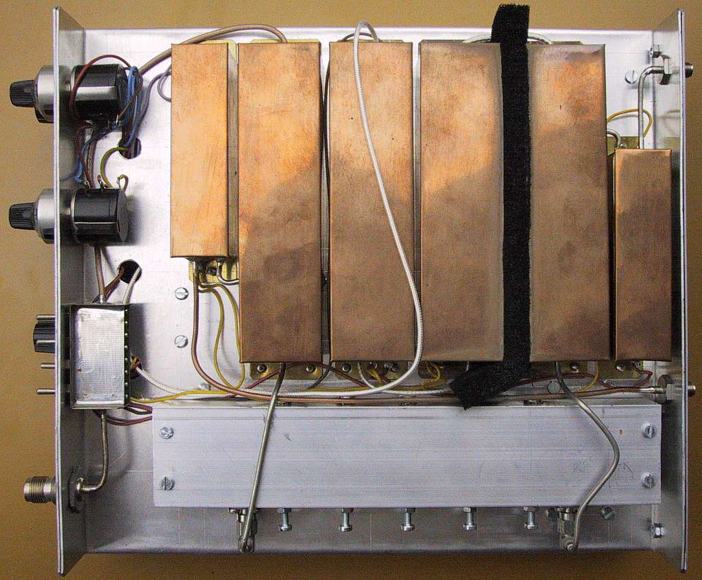
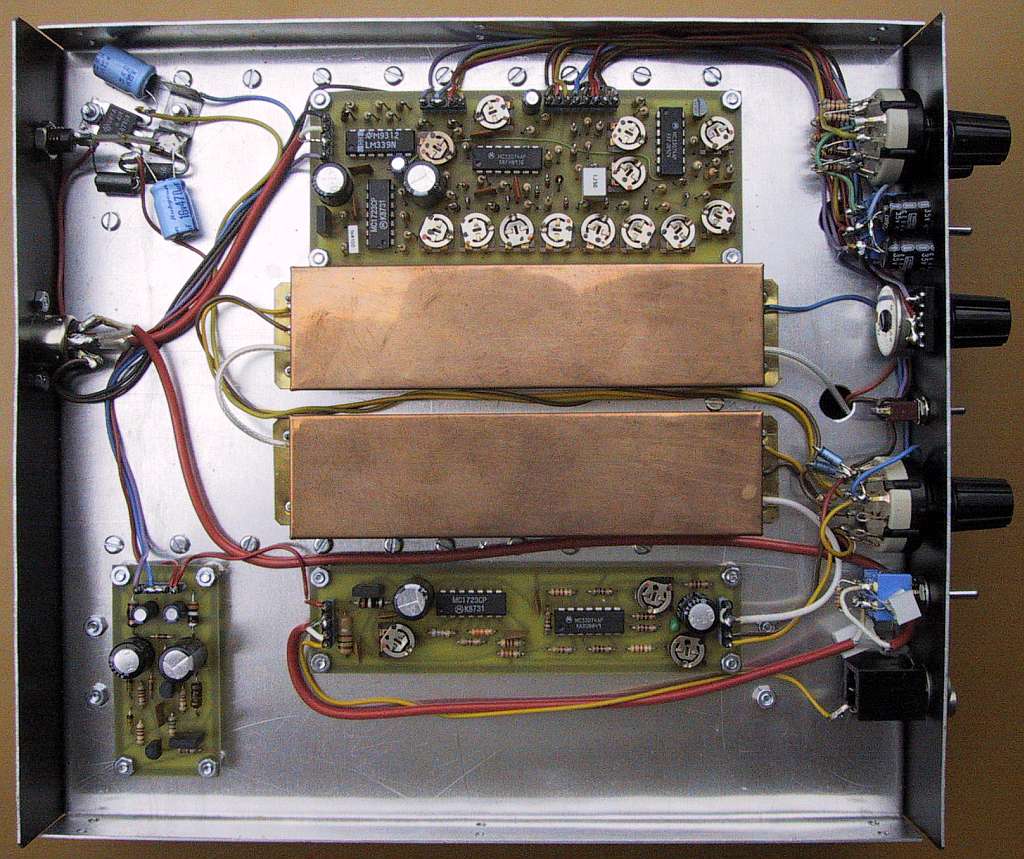
While positioning the different modules on the baseplate, care should be taken that the mounting screws do not interfere with the modules on the other side. The cavity is hold in place by a pair of screws on each "cold" end, so that no metal parts enter the "hot" central part of the filter. The front panel is connected to the baseplate with the TNC connector, toggle switches and Helipots, so no additional screws are necessary. On the other hand, the back panel is connected with four M3 screws in addition to the SMA connectors.
Finally, it is convenient that all display connections are brought to a single multi-pole connector on the back panel. The suggested 6-pole, 270-degree DIN connector is shown on Fig.20. Different displays therefore only require special cables. The same display connector also carries the +12V supply for a storage/normalizer unit or marker generator.
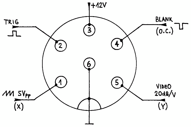
Fig.20 - Display connector.
13. Alignment and checkout
Before starting the construction of a complex piece of test equipment like a spectrum analyzer, some simpler test equipment should be available as well as enough practical experience to efficiently use the latter. Besides a conventional analog AVO-meter (digital AVO-meters are useless for tuning), a grid-dip meter, a microwave frequency counter up to at least 4GHz and a microwave power sensor should be available. Last but not least, the oscilloscope to be used as the display of the spectrum analyzer should also be available.
The construction of the spectrum analyzer should start with the most difficult part: the VCOs described in [1] and [2]. Both VCOs have to be checked for the frequency coverage and output power. In fact it makes sense to build two wide-band VCOs. The best VCO is installed in the spectrum analyzer. The leftover VCO can still be used in other test equipment, like a harmonic converter that extends the coverage of a spectrum analyzer, to be described in a later article.
When both VCOs are operating correctly, the remaining modules can be built except the LC and crystal filters. The third mixer and logarithmic detector can be aligned and checked with a grid-dip meter. The operation of the sawtooth generator, linearization circuit and several selectors and potentiometers can be checked with the oscilloscope that will be used for display. All the trimmers in the linearization should be set to their "cold" ends.
The cavity bandpass filter is the unit that is most difficult to align without complex test equipment. The tuning screws are initially set about 1...2mm above the "hot" ends of the resonators. The narrow-band VCO is set to 2.03GHz with a frequency counter while the wide-band VCO is sweeping the whole frequency band. The cavity filter can then be tuned to the characteristic "DC peak" of all RF spectrum analyzers.
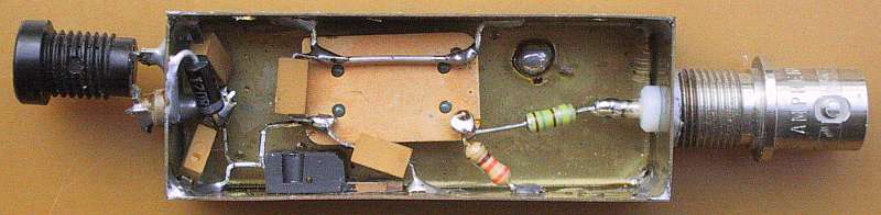
When the "DC peak" is found and the cavity bandpass is roughly tuned to the correct frequency, an initial checkout of the spectrum analyzer can be performed. A short antenna connected to the RF input will provide many peaks around 100MHz (FM broadcast) and 900MHz (GSM). Even better is a simple 100MHz test source built with a 100MHz ECL crystal oscillator, as shown on Fig.21.
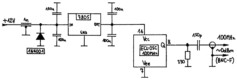
Fig.21 - 100MHz test source.
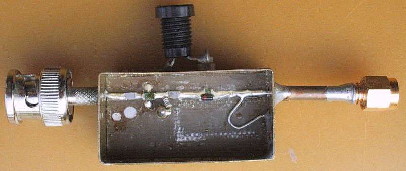
The adjustment of the linearizer requires several signals on known frequencies. The simplest solution is a comb generator (shown on Fig.22) that provides many equally-spaced harmonics of the same fundamental frequency. The usual image on the display is rather dense lines between 700MHz and 1000MHz, while the spacing of the lines gradually increases both towards lower frequencies and even more towards higher frequencies. The eight trimmers in the linearizer are then adjusted to obtain equally spaced lines across the whole display. If the adjustment range of the trimmers is not sufficient, other resistors in the circuit may be changed to match the response of the varactors in the wide-band VCO.
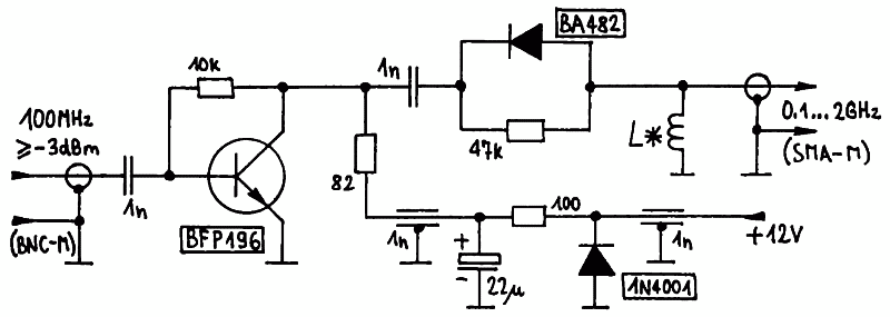
Fig.22 - Comb generator up to 2GHz.
When the spectrum analyzer is operating correctly with a 4MHz IF bandwidth, additional LC and crystal filters can be built. Finding suitable filter crystals is not simple. Cheap "clock" or "baud-rate" crystals were found useless, since they have many spurious resonances close to the main resonant frequency. Such crystals may still provide some useful performance in narrow SSB filters, but their response is badly distorted in wide (B=50kHz) filters for spectrum analyzers.
The only reliable crystals are those found in old 35kHz-wide filters for 50kHz FM-channel spacing. These crystal filters were usually built for a center frequency of 10.7MHz. One filter contains four different crystal pairs. Therefore two identical crystal filters have to be disassembled to obtain enough crystals for four spectrum analyzers...
Both crystal and LC filters are simply adjusted on the "DC peak", when the remaining parts of the spectrum analyzer are already operating. The alignment of LC filters is straightforward and the desired response is obtained easily.
On the other hand, the alignment of the crystal filter is very demanding. Each filter stage has to be aligned independently while the remaining three crystals are shorted with 100ohm resistors. A symmetrical response of a single filter stage is sought with the capacitive trimmer. Next the coil is adjusted to obtain the broadest peak, of course with the current in the PIN diode turned off. This procedure has to be repeated several times for each stage, since the two adjustments interact.
After the LC and crystal filters are roughly adjusted, the two trimmers in the third mixer module can be adjusted. The mixer linearity is adjusted with a strong (around -10dBm) signal on the first mixer input. Setting the resolution bandwidth to 150kHz, some spurious responses may be visible +/-2MHz around the desired signal. These spurious responses should be minimized by adjusting the mixer linearity. Finally, the gain of the 70MHz amplifier is set so that the front-end noise just overrides the detector noise with the 150kHz IF filter.
At the end, there are many fine adjustments to be performed. All IF filters should be aligned to the same frequency and same insertion loss. If the noise floor changes with frequency, then the symmetry of the first mixer should be improved by small drops of solder on the UT-085 balun. The remaining trimmers in the sawtooth and linearization module have to be adjusted so that the display matches the selected span width.
Of course, a number of fine adjustments are only performed after spotting problems in the practical use of the spectrum analyzer. Some adjustments, like the precise impedance matching of the wide-band VCO to the first mixer, can only be performed with a tracking generator, to be described in a future article. In any case it is assumed that the builder is familiar with the theory of operation of a spectrum analyzer, since in this case most troubleshooting can be performed with the same spectrum analyzer.
Original full-size drawings

References:
[1] Matjaz Vidmar: "Rauscharmer, breitbandiger Mikrowellen VCO", pages 26-35/4-98, AMSAT-DL Journal.
[2] Matjaz Vidmar: "Wideband & Low-Noise Microwave VCO", pages 210-225/4-98, VHF-Communications.
* * * * *