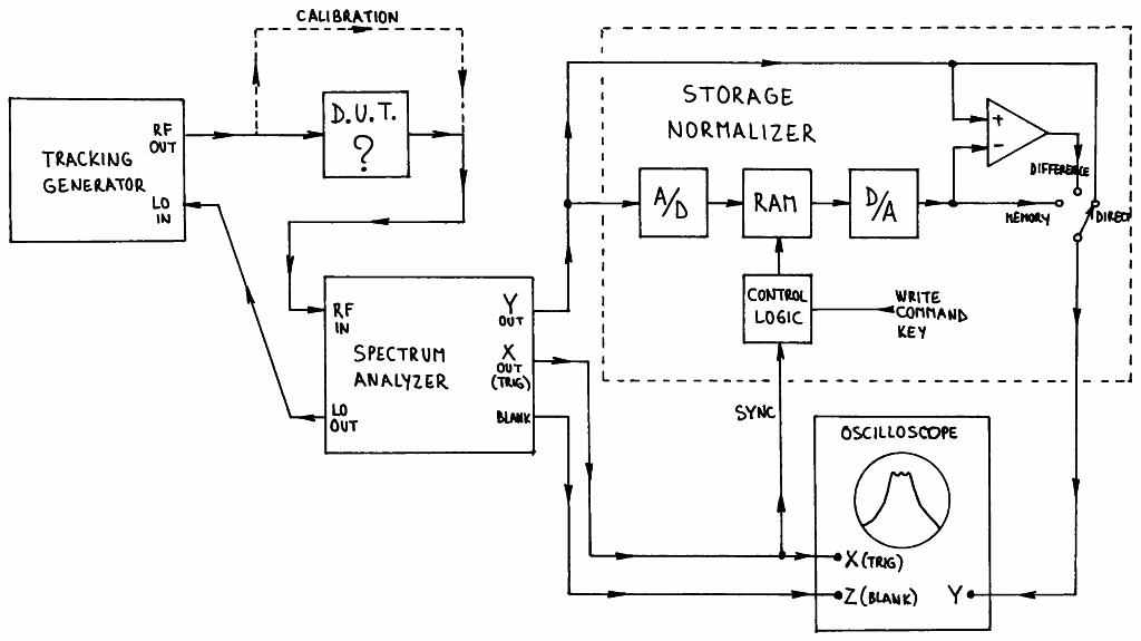
Fig.1 - Principle of operation of a storage-normalizer.
(VCO)
(SA)
(TG)
(HC)
(SN)
(MC)
(LCD)
(HOME)
Storage-Normalizer for Spectrum Analyzers
Matjaz Vidmar, S53MV
1. Displays for spectrum analyzers
Spectrum analyzers usually produce large quantities of information that can be properly represented only on a fully graphic display. The latter can be a simple oscilloscope CRT display, a raster-scan CRT or a dot-matrix LCD. Many older spectrum analyzers were equipped with delicate and difficult-to-use CRTs with a special storage screen. Newer spectrum analyzers have digital video memories and usually provide a hardcopy option, either with a built-in printer or through a general computer interface.
Unfortunately, new display technologies do not necessarily mean improvements of the overall instrument performance. In particular, in the case of radio-frequency spectrum analyzers, all engineers appreciate the good old analog oscilloscope displays. New spectrum analyzers, including the highest-priced models, all include digital displays that have both too low resolution and too slow display update.
Of course, the best solution is to have both analog and digital display technologies available in a single instrument. An older spectrum analyzer or a homemade instrument with an analog oscilloscope display can easily be upgraded with an additional storage-normalizer unit. Since the latter can be switched in and out as required by the particular measurement, it allows the advantages of both display technologies in a single instrument.
A storage-normalizer is particularly useful while using a tracking generator as shown on Fig.1. In the latter case, the response of the tracking generator, spectrum analyzer and other test equipment is stored in digital memory during system calibration. The response of the device-under-test (DIRECT) can then be quickly compared with the stored system response (MEMORY). Since most spectrum analyzers provide a logarithmic video signal (usually 10dB per division), a simple subtraction of the system response from the measured trace (DIFFERENCE) removes any system influence on the measured device response.
Fig.1 - Principle of operation of a storage-normalizer.
2. Storage-normalizer design
A simple storage-normalizer is described in this article, to be used with the spectrum analyzer described in [1] or [2] or other similar instruments. Since the narrowest resolution bandwidth of the above-mentioned spectrum analyzer is only 10kHz, very slow frequency sweeps are usually not used. A digital storage is therefore not required for faster frame refresh at very slow sweep times.
The design of the storage-normalizer is much simplified since the display always operates at the same sweep frequency as the spectrum analyzer. All required clock and address signals are generated by simple and fast hardware logic in place of a much slower microcontroller. Fast A/D and D/A converters and a sufficiently large memory allow high-quality images to be stored in the video memory.
The video bandwidth of the spectrum analyzer ([1] or [2]) amounts up to 500kHz without any video filtering. To avoid any video degradation, a sampling frequency of 1MHz was selected. A sampling frequency of 1MHz is far too high for most microcontrollers. Therefore a simple control logic with 74HCxxx circuits generates all required clocks and addresses.
The dynamic range of the logarithmic detector amounts to almost 100dB. Inexpensive 8-bit A/D and D/A converters therefore allow a resolution of about 0.4dB for the storage-normalizer. A resolution of 0.4dB is comparable to the accuracy of the 10-stage logarithmic detector presented in [1] or [2].
The A/D and D/A converters as well as the video memory are shown on Fig.2. The A/D converter TDA8703 is a 8-bit flash A/D converter that allows sampling frequencies up to 30MHz. Flash A/D converters include a comparator for each step of their transfer function, in total 255 comparators in a 8-bit A/D converter. Their main advantage is very fast operation. Also, flash A/D converters do not require a critical sample-and-hold circuit on the analog input.
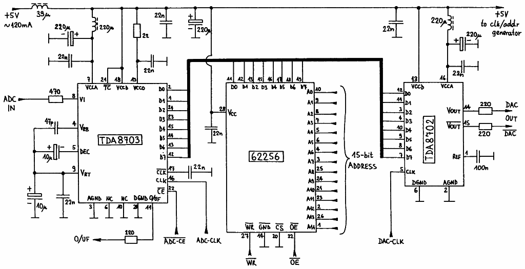
Fig.2 - A/D and D/A converters and video memory.
The TDA8703 has three-state outputs to be connected directly on an 8-bit data bus. The O/UF (over/underflow) is an additional output that goes high whenever the input-signal level is too low or too high, in other words outside the normal operating range of the A/D converter. While testing the circuit of the storage-normalizer it may be useful to connect a LED from the O/UF output to ground, of course through the 220ohm current-limiting resistor.
The 62256 is a 32768-byte static CMOS RAM. At a sampling frequency of 1MHz it can store about 32ms of video signal. The storage-normalizer is intended to be used at a sweep speed of 2ms/division for a total sweep time of 20ms, resulting in 20000 samples or 20000 bytes to be stored in the video memory. The 62256 has eight common input-output pins D0...D7, that can be tri-stated and connected directly to an 8-bit data bus.
The TDA8702 is a fast 8-bit D/A converter. It includes an internal 8-bit latch on the digital inputs. Data transfer is triggered by the DAC-CLK, so that the same data bus can also be used for other purposes. The TDA8702 has two complementary analog outputs. Both outputs are used in the storage-normalizer to further reject noise and voltage variations on the +5V supply line.
The A/D and D/A converters as well as the memory require several steering signals. The clock/address generator is shown on Fig.3. All clocks run at 1MHz, but have different pulsewidths and phases. All clocks are obtained from a 8MHz crystal oscillator driving a 8-bit shift register (74HC164). The shift register is connected as a frequency divider by 8. The different clocks are obtained from the 74HC164 outputs through a few NAND gates (two 74HC00).
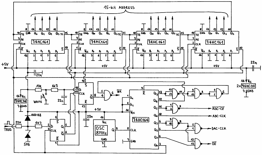
Fig.3 - Clock/address generator.
The A/D converter TDA8703 performs one conversion for each ADC-CLK pulse. The outputs of the TDA8703 are then enabled by the /ADC-CE signal. Writing to the memory is enabled with /WR while reading from the memory is enabled by /OE. Finally the byte from the memory is copied into the D/A converter TDA8702 with DAC-CLK. When all clocks are disabled, the output Q0 of the 74HC164 increments the address counter.
The address counter includes four synchronous counters 74HC161. The TRIG pulse coming from the spectrum analyzer signals the start of the sweep. After the TRIG pulse is "cleaned" in a D-flip-flop (one half 74HC74), it resets the address counter. The address counter supplies a 15-bit address to the memory. The last counting stage (Q3 of the last 74HC161) is used to stop the address counter until the next trigger pulse.
Writing the video data to memory is enabled manually by depressing the WRITE key. The write command is synchronized to the display sweep with a D-flip-flop (second half 74HC74). In this way one or more whole sweeps are written to the memory regardless of the WRITE-key contact bouncing. The WRITE command enables the /WR clock. The latter remains in its inactive (high) state when writing is not enabled.
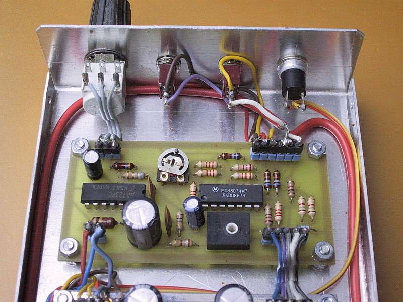
The digital memory requires an analog interface as shown on Fig.4. The latter is used to adjust the A/D and D/A signal levels to the values used between the spectrum analyzer and oscilloscope display (20dB/V, impedance 680ohm). Further, the analog interface includes a circuit with operational amplifiers to compute the difference between the direct video signal and memory content.
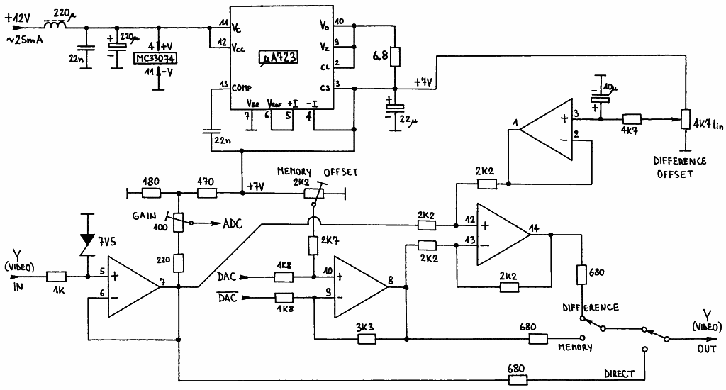
Fig.4 - Analog interface.
The analog interface includes a quad operational amplifier MC33074. The first op-amp (pins 5,6,7) is a voltage follower for the input signal. The A/D converter gets part of this signal through a resistive divider. The second op-amp (pins (8,9,10) amplifies the output of the D/A converter to the same level as available directly from the spectrum analyzer. The third op-amp computes the signal difference. Finally, the fourth op-amp (pins 1,2,3) operates as a voltage follower for the DIFFERENCE-OFFSET control voltage.
The four operational amplifiers run on a +12V supply, since the input and output video-signal voltages usually range between 1V and 6V. A stable +7V reference voltage is provided by the uA723 regulator. On the other hand, the A/D and D/A converters as well as the memory require a +5V supply voltage. The overall power supply is shown on Fig.5 providing +5V for the digital memory +12V for the analog interface.
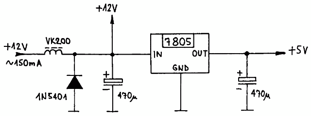
Fig.5 - Power supply.
3. Storage-normalizer assembly and alignment
The wiring of the storage-normalizer modules is shown on Fig.6. The spectrum analyzer provides four signals: video (Y-deflection), triggering (TRIG), blanking (BLANK) and sawtooth (X-deflection). The storage-normalizer only affects two signals: the video signal is being processed while the TRIG signal is used for synchronization of the address counter.
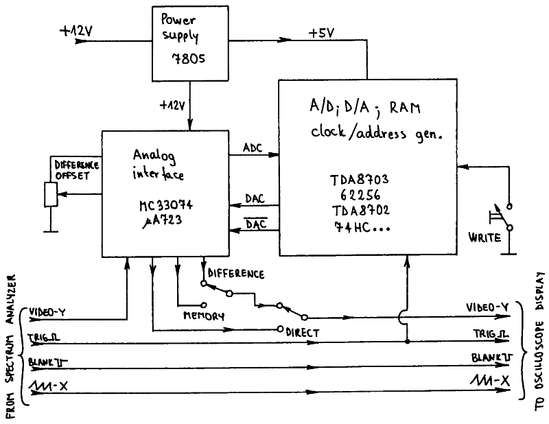
Fig.6 - Storage-normalizer wiring diagram.
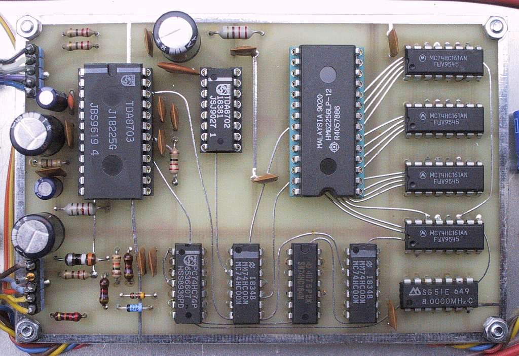
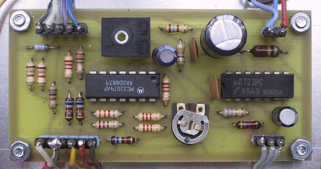
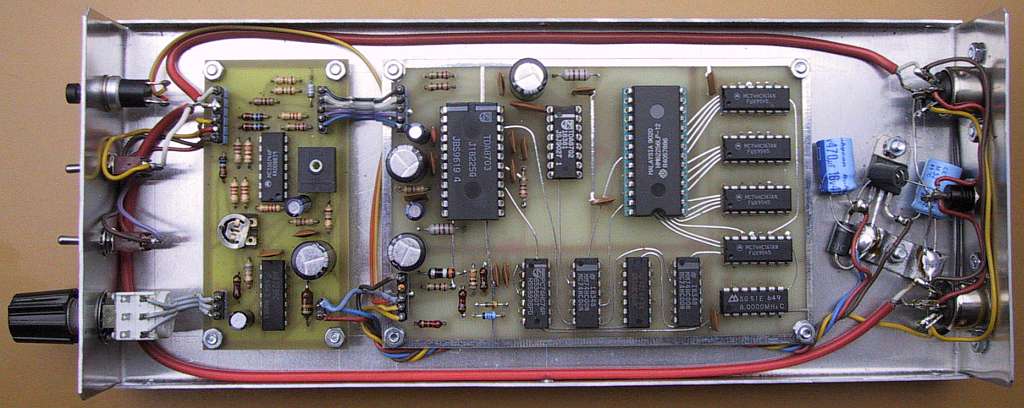
The storage-normalizer is built on two printed-circuit boards except for the power supply from Fig.5. The latter is built around the 7805 regulator and +12V supply connector. The digital part of the storage-normalizer (A/D and D/A converters, memory and clock/address generator) are built on a double-sided printed-circuit board with the dimensions of 120mmX80mm as shown on Fig.7. The analog interface is built on a single-sided printed-circuit board with the dimensions of 80mmX40mm as shown on Fig.8. Both circuit boards are etched on 1.6mm-thick glassfiber-epoxy laminate FR4.
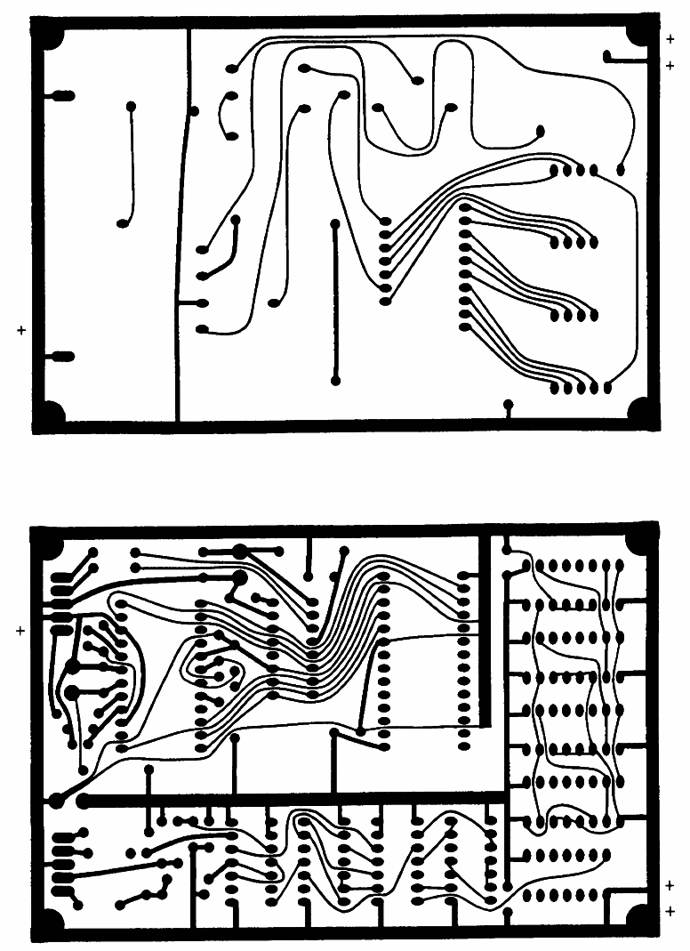
Fig.7 - Digital-memory circuit board (150dpi).
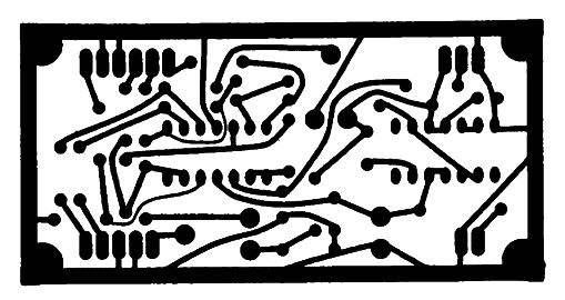
Fig.8 - Analog-interface circuit board (150dpi).
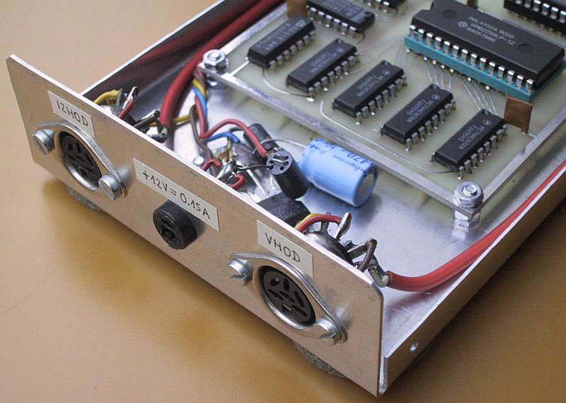
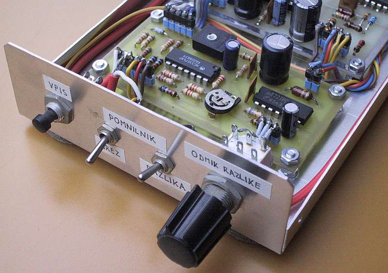
The storage-normalizer module location is shown on Fig.9. The storage-normalizer has the same depth (240mm) as the spectrum analyzer [1] or [2]. The width is 100mm while the height is only 32mm, since all modules are located in a single plane. The bottom of the box is simply a piece of 1mm thick aluminum sheet, bent in the form of an "U". The cover is a similar "U" made from 0.6mm thick aluminum sheet.
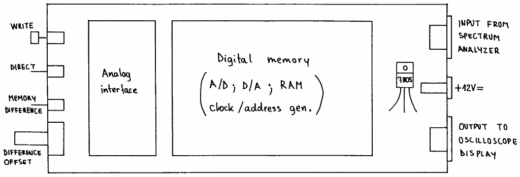
Fig.9 - Storage-normalizer module location.
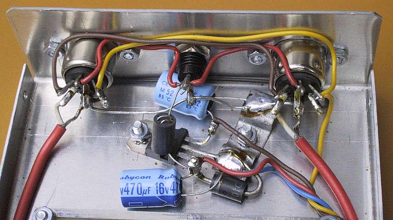
The 7805 regulator is bolted to the bottom plate for heatsinking purposes. The two 470uF electrolytic capacitors, VK200 RF choke and 1N5401 diode are simply soldered between the +12V supply connector and the leads of the 7805 regulator. The overall current drain amounts to about 150mA.
Although the storage-normalizer is a low-frequency video circuit, the analog interface requires a few alignments to make best use of the available dynamic range of both A/D and D/A converters. Of course the storage-normalizer should perform some useful function without any alignment (with both trimmers and potentiometer in central position) and this can be checked immediately with the oscilloscope display.
In the storage-normalizer the correct input signal level to the A/D converter should be set first. For this purpose the spectrum analyzer is tuned to represent a wide and high peak across the whole display in the DIRECT mode. Next the storage-normalizer is switched to DIFFERENCE and the WRITE key is kept depressed. The GAIN trimmer is then adjusted to obtain a straight line on the oscilloscope display.
If a straight line can not be obtained, the input signal level is probably outside the range required by the TDA8703. This can be readily checked with a LED connected to the O/UF output. The most efficient counter-measure is to correct the DC offset of the video amplifier inside the spectrum analyzer. Since the LED is no longer required after the video signal levels in the spectrum analyzer and storage-normalizer are adjusted correctly, the LED is not installed on the front panel.
After the trimmer GAIN is adjusted correctly, the storage normalizer is switched alternatively in the DIRECT and MEMORY modes. The trimmer MEMORY OFFSET is then adjusted so that there is no observable difference between the DIRECT and MEMORY displays. Finally, the potentiometer DIFFERENCE OFFSET is a front-panel command and is set accordingly to the type of measurement that is performed: spectrum analyzer alone, tracking generator or different devices under test with insertion loss or gain.
While using the described simple storage-normalizer one should however understand that the latter has no information about the settings of the spectrum analyzer. If the central frequency, sweep width or sweep time are changed, the information stored in the storage-normalizer probably becomes useless. The whole system should be then calibrated again, writing new information in the storage-normalizer memory.
Original full-size drawings

References:
[1] Matjaz Vidmar: "Spectrum analyser 0...1750MHz", pages 2-30/1-99, VHF-Communications.
[2] Matjaz Vidmar: "Spektrum-Analyzer von 0 bis 1750MHz, Teil 1: Aufbau der Baugruppen", pages 18-30/4-99, "Spektrum-Analyzer von 0 bis 1750MHz, Teil 2: Anzeigebaugruppen und Abgleich", pages 18-29/1-00, AMSAT-DL Journal.
* * * * *