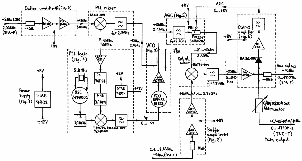
Fig.1 - Tracking-generator block diagram.
(VCO)
(SA)
(TG)
(HC)
(SN)
(MC)
(LCD)
(HOME)
Tracking Generator 100kHz...1750MHz
Matjaz Vidmar, S53MV
1. Tracking generator principles
A basic and very useful addition to a spectrum analyzer is a tracking generator. A tracking generator produces a RF signal on the exact frequency where the spectrum analyzer is receiving at the same time. A tracking generator therefore allows testing many passive and active RF circuits that do not produce any RF signals on their own, like filters, amplifiers etc. With an additional directional coupler or bridge, reflection measurements can be performed in the whole frequency range covered by the spectrum analyzer.
The simplest tracking generator is a wide-band noise source, since part of the noise power always falls in the instantaneous receiving bandwidth of the spectrum analyzer. Since the noise figure of typical spectrum analyzers is rather high, in the range around 15-20dB, the required ENR (excess noise ratio) of the noise source is very high. Further, the dynamic range of noise measurements is quite limited, since the device under test and the input of the spectrum analyzer are both loaded with much larger power levels than are actually being measured. Finally, noise measurements always require some averaging (video filtering) due to the random nature of noise signals.
To avoid the drawbacks of noise measurements, almost all manufacturers offer tracking generators that produce a coherent sinusoidal signal on the receiving frequency of the spectrum analyzer, either built-in or as separate units. A tracking generator usually does not include very expensive components. Nevertheless, commercial tracking generators may be quite expensive, up to one quarter of the cost of the spectrum analyzer. Therefore it makes sense to build companion tracking generators even for commercial spectrum analyzers.
A tracking generator designed to operate with the spectrum analyzer described in [1] or [2,3] will be described in this article. Since most commercial spectrum analyzers use similar frequencies for the first IF (usually in the range 2...3GHz), many of the described circuits are also useful to build a tracking generator for a commercial spectrum analyzer. Of course, the exact circuit diagram of a tracking generator should match the frequency conversions in the corresponding spectrum analyzer.
A tracking generator obtains its output signal exactly in the opposite way the different frequency conversions are made inside the spectrum analyzer. A tracking generator therefore requires the signals from all variable oscillators (VCOs) inside the spectrum analyzer. Most spectrum analyzers therefore have the signals of the first, second and sometimes even third local oscillator accessible on suitable RF connectors on the front panel or sometimes back panel.
The spectrum analyzer, described in [1] or [2,3], includes two variable oscillators (VCOs) for the first and second conversion. A suitable tracking generator requires the same conversion processes in the reverse direction, as shown on the block diagram on Fig.1. First, the tracking generator should add the frequency of the second IF (around 70MHz) to the second VCO at 2.03GHz (+/-10MHz). The sum is a signal at the first IF around 2.1GHz. The latter is afterwards subtracted from the frequency of the first VCO (2.1...3.85GHz). An automatic-gain-control (AGC) loop is used to stabilize the output-signal amplitude over the whole frequency range 100kHz...1750MHz.
Fig.1 - Tracking-generator block diagram.
Frequency summation and subtraction can be performed in different ways: using mixers and filters or with phase-locked loops (PLLs). All signals inside the tracking generator have relatively high levels. Unwanted mixing products should be monitored carefully. On the other hand, thermal noise is not very important if compared to the design of a spectrum analyzer or other receivers. Finally, suitable shielding should be provided to avoid unwanted signal paths as well as using buffer amplifiers to provide the required separation wherever necessary.
In the described tracking generator, the first frequency summation 70MHz and 2.03GHz is performed by a phase-locked loop. The second conversion (subtraction) of the 2.1GHz first IF from the first LO 2.1...3.85GHz is performed by a balanced mixer followed by a low-pass filter on the output. Two identical buffer amplifiers are used for both VCO signals to prevent any interference from the tracking generator back into the spectrum analyzer.
The AGC sets the output-signal level to about 1mW (+0dBm). The latter can be further attenuated down to -40dBm when required on the main tracking-generator output. An auxiliary, fixed -10dBm output is provided for a frequency counter.
The described tracking generator includes nine shielded RF modules and a power supply. Some modules are identical to those in the spectrum analyzer: the PLL mixer is identical to the second mixer in the spectrum analyzer while the output mixer is identical to the first mixer in the spectrum analyzer. The output attenuator with four 10dB steps is identical to the input attenuator in the spectrum analyzer. Of course, the description of all identical modules will not be repeated.
2. Buffer amplifiers
The tracking generator includes two identical buffer amplifiers for the signals of both VCOs in the spectrum analyzer. The buffer amplifiers have two main functions: amplify the signals of both VCOs to about +13dBm to drive both mixers and prevent any signals from the tracking generator returning back in the VCOs and mixers of the spectrum analyzer.
The circuit diagram of (one) buffer amplifier is shown on Fig.2. The buffer amplifier includes a -10dB attenuator and two amplification stages. The input attenuator allows a good input impedance match even with the power turned off. Even more important, the input impedance does not change much after turn-on, so that the frequency pulling of both VCOs inside the spectrum analyzer is kept small enough.
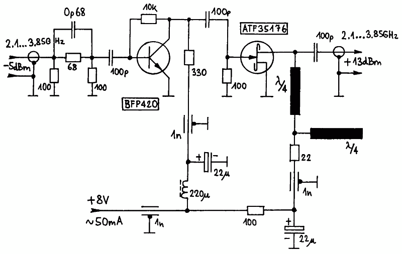
Fig.2 - Buffer amplifier.
The input attenuator is followed by a simple amplifier stage with a BFP420 transistor. The high-frequency gain decay of the latter is partially compensated by the 0.68pF capacitor in parallel to the 68ohm resistor in the attenuator. The output stage uses an ATF35176 HEMT to obtain the required output power. The output of the buffer amplifier is connected through a short piece of UT-085 semirigid cable, used at the same time as a balun inside the balanced mixer.
Both amplifier stages are supplied with +8V through suitable resistors and feed-through capacitors. The operating point of the output stage may change due to the Idss tolerances of the ATF35176 HEMT, but these changes have little effect on the performance of the amplifier. The drain voltage (Uds) may be anywhere in the range 2...3.5V.
3. PLL for 2.1GHz
The first signal-processing step inside the tracking generator is the addition of the second VCO frequency and the second IF. Of course, the tracking generator should contain its own oscillator to generate a signal on the second IF around 70MHz. The two frequencies could be simply added in a mixer. Unfortunately, the filtering of the output signal would require a complex cavity bandpass filter to remove the image at 1.96GHz as well as the second VCO leakage at 2.03GHz. Further, an AGC circuit would be required to avoid overdriving the mixer.
The same task can be performed by a phase-locked loop with its own VCO operating at the output frequency of 2.1GHz. A small fraction of the latter is mixed with the second VCO signal at 2.03GHz coming from the spectrum analyzer. The difference of the two frequencies is compared with the nominal second IF value and the result of this comparison is used to correct the frequency of the 2.1GHz VCO. The 2.1GHz signal does not require any further filtering. However, the PLL should be designed to achieve lock reliably and to track the 2.03GHz signal even when the frequency of the second VCO in the spectrum analyzer is swept.
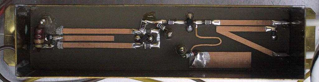
The VCO for 2.1GHz (shown on Fig.3) is very similar to the second VCO in the spectrum analyzer operating at 2.03GHz. Since only a relatively narrow frequency range around 2.1GHz has to be covered, a single tuning varactor BB833 is sufficient in the central finger of the interdigital bandpass. A BFP183 transistor is used as the active device inside the VCO, while an INA10386 MMIC is used as the output buffer. A directional coupler takes a small part of the output signal (around -5dBm) for the PLL mixer.
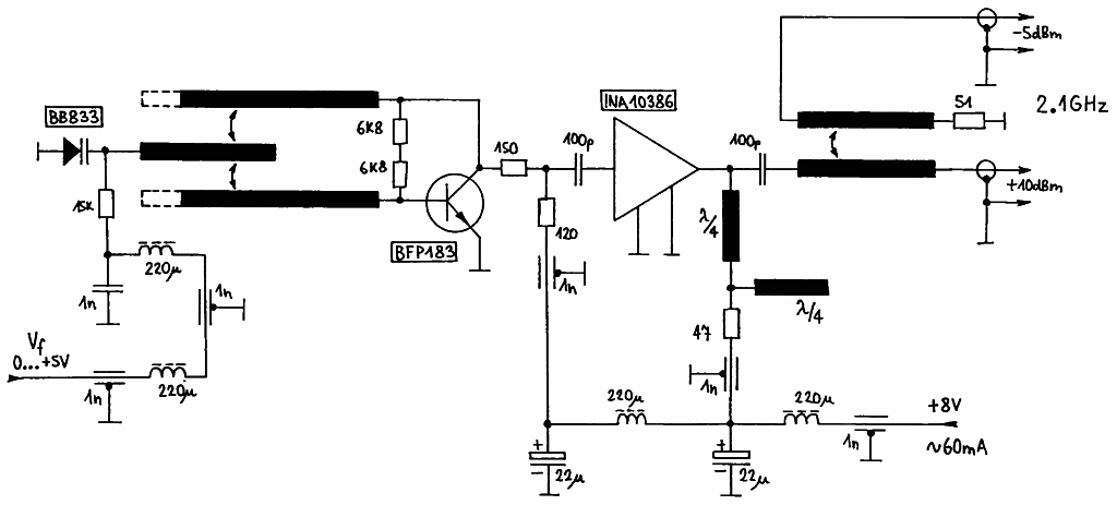
Fig.3 - VCO for 2.1GHz.
The VCO for 2.1GHz is built on an identical printed-circuit board as the narrow-band VCO in the spectrum analyzer. Besides a different varactor, both the collector and base microstrips are shortened by about 2mm at their open ends to achieve a higher operating frequency. The control-voltage low-pass network has to be designed carefully to allow a fast response of the control loop.
The PLL mixer is identical to the second mixer in the spectrum analyzer. The -5dBm VCO output is connected to the 2.8GHz low-pass inside the mixer module, while the buffer amplifier is connected to the semirigid balun. The frequency difference (around 70MHz) is taken from the 800MHz low-pass.
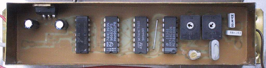
The comparison between the nominal value 70MHz and the actual frequency difference is performed by the PLL logic shown on Fig.4. The PLL logic includes a reference crystal oscillator, two dividers for the reference frequency and the actual frequency difference and a charge-pump frequency/phase comparator.
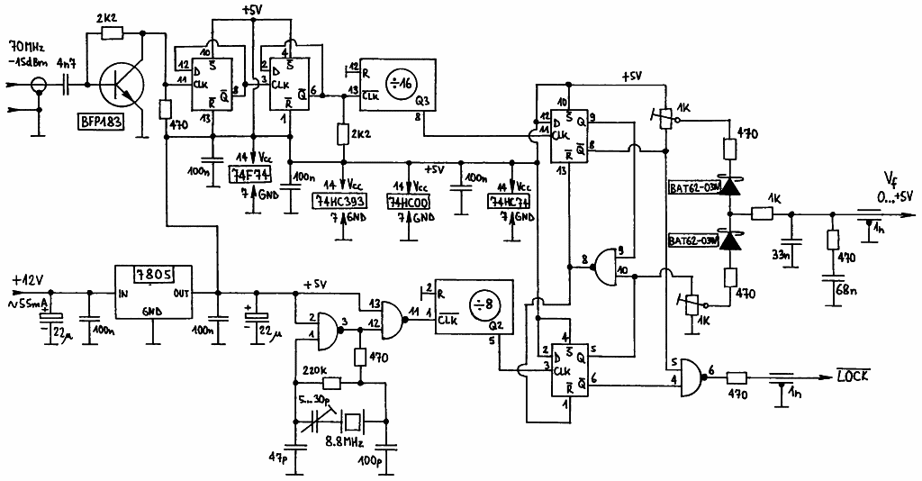
Fig.4 - PLL logic.
While the PLL is unlocked, the actual frequency difference may deviate substantially from the nominal value around 70MHz. An upper limit of about 140MHz is set by the input divider 74F74 with the suggested BFP183 driver. The frequency difference is divided by 64, while the 8.8MHz reference is divided by 8. The 1.1MHz comparison frequency allows fast tracking of the narrow-band VCO in the spectrum analyzer even when the frequency of latter is swept.
The reference crystal-oscillator frequency is selected to 1/8 of the second IF of the spectrum analyzer. Of course, the exact value depends on the components used in the spectrum analyzer, in particular the crystal used in the third conversion (usually 60.000MHz) and crystal filter (usually 10.700MHz). For a nominal second IF value of 70.700MHz a reference crystal oscillator at 8837.5kHz is required.
The output-voltage (Vf) range of the charge-pump frequency/phase comparator (max 0...+5V) usually has to be further reduced by the two 1kohm trimmers. The frequency difference should never become too large (140MHz limit imposed by the 74F74 divider) nor should the PLL be allowed to lock onto the image response of the mixer. The charge pump with the two schottky diodes BAT62-03W is followed by a RC low-pass network, defining the settling time and stability of the feedback loop.
4. Output mixer, amplifier and AGC
The second signal-processing step is the subtraction of the 2.1GHz frequency (first IF of the spectrum analyzer) from the first LO frequency 2.1...3.85GHz. All unwanted spurious conversion products from a correctly-designed mixer can simply be removed by a low-pass filter on the output, leaving only the desired signal in the frequency range 0...1750MHz. On the other hand, it is very difficult to build a PLL covering such a wide frequency range.
The output mixer is identical to the first mixer in the spectrum analyzer. The latter module includes a 1.75GHz low-pass. The wide-band-VCO signal (2.1...3.85GHz) is fed through a buffer amplifier directly to the semirigid balun of the output mixer. No further processing is required, since the harmonics of the first spectrum-analyzer LO do not cause any harmful spurious frequencies in the tracking generator.
On the other hand, the tracking generator is sensitive to the harmonics of the 2.1GHz first-IF signal. The latter may cause spurious mixing products in the output-frequency range 0...1750MHz. Therefore, any harmonics of the 2.1GHz signal have to be removed. Further, the 2.1GHz signal level has to be controlled carefully to avoid mixer nonlinearities.
The 2.1GHz harmonics are removed by a 2.8GHz low-pass filter, followed by a PIN-diode attenuator to set the signal level for the mixer. Both circuits are included in the AGC module shown on Fig.5. The PIN attenuator is followed by another 2.8GHz low-pass in the output mixer module.
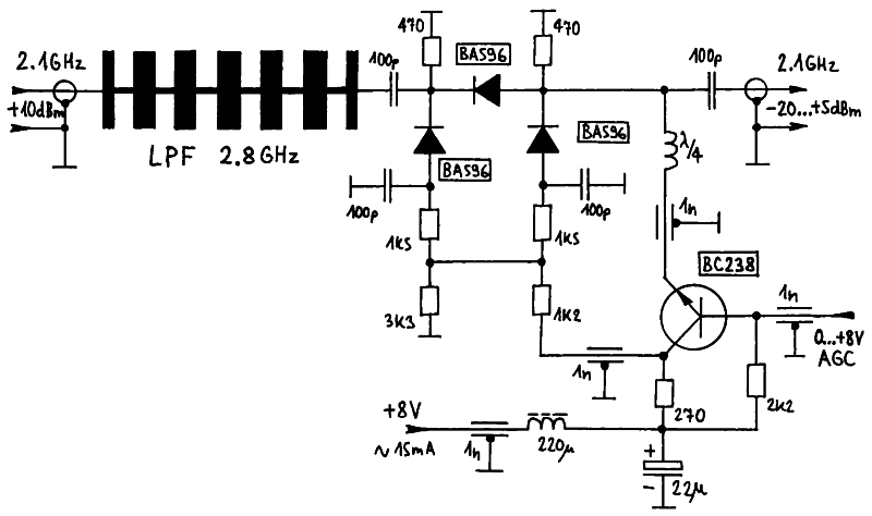
Fig.5 - AGC.
The PIN attenuator includes three PIN diodes BA596 connected in a PI network. The BC238 transistor feeds all three PIN diodes with suitable DC currents to keep the input and output impedances stable while adjusting the attenuation. The AGC control voltage spans from zero to +8V. Minimum attenuation is achieved at +8V while zero voltage provides maximum attenuation.
Since the output mixer operates in the linear region, the output signal is relatively weak, around 10uW or -20dBm. To increase the output signal level and drive the AGC detector, an output amplifier is required as shown on Fig.6. The latter is built with an INA10386 MMIC that provides 26dB gain and an output power of more than +10dBm in the whole frequency range up to 1750MHz.
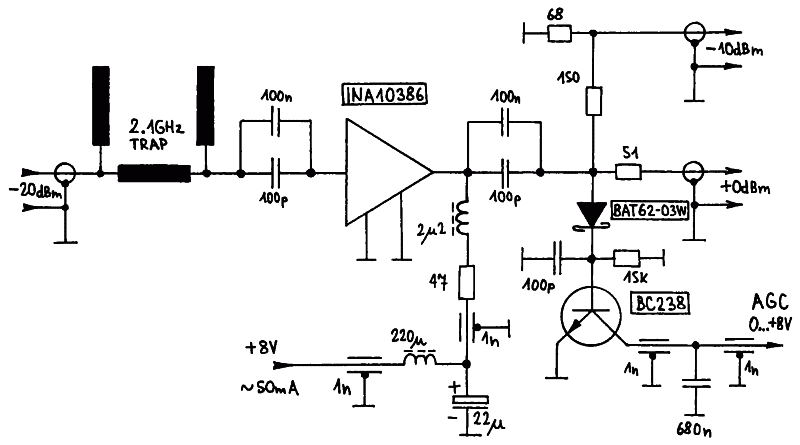
Fig.6 - Output amplifier.
The INA10386 MMIC amplifier requires DC decoupling capacitors on both the input and output. The latter limit the lower end of the frequency range of the tracking generator to about 100kHz. Each coupling capacitor includes a parallel connection of two SMD capacitors: first a low-loss, 100pF NP0 0805 capacitor is soldered on the printed-circuit board and afterwards a 100nF, lossy Z5U 1206 capacitor is soldered across the 100pF capacitor.
The AGC detector (schottky diode BAT62-03W) is connected directly to the output of the INA10386 amplifier. The BC238 transistor operates as the AGC feedback amplifier, while the time constant of the feedback is set by the 680nF capacitor. Thanks to the AGC action, the output amplifier behaves as a voltage source. The main output (+0dBm) therefore requires a 51ohm series resistor. The 150ohm and 68ohm resistors allow an auxiliary -10dBm output and provide a DC path to ground for the AGC detector.
The main output of the tracking generator includes a step attenuator to decrease the output signal level down to -40dBm in four 10dB steps. The design of this attenuator is identical to the attenuator used on the input of the spectrum analyzer. Due to the non-ideal frequency response of the latter, better measurement accuracy can be achieved with the auxiliary -10dBm output, especially for wide-band measurements.
5. Construction tips
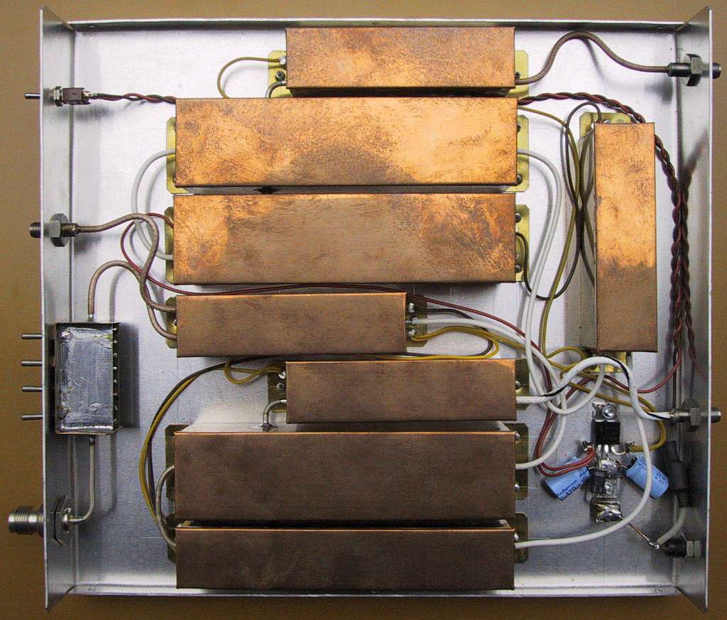
The described tracking generator is built in a similar way as the corresponding spectrum analyzer, described in [1] or [2,3]. All modules are installed in shielded boxes made from 0.5mm thick brass sheet. Most modules require a +8V supply voltage obtained from the 7808 regulator shown on Fig.7. The PLL logic has its own 7805 regulator inside the module and requires a +12V external supply. The tracking generator is equipped with an ON/OFF switch on the front panel to allow an immediate check of the signals shown on the spectrum-analyzer display.
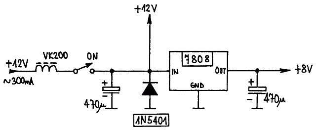
Fig.7 - Power supply.
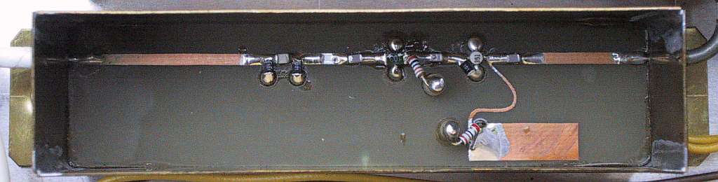
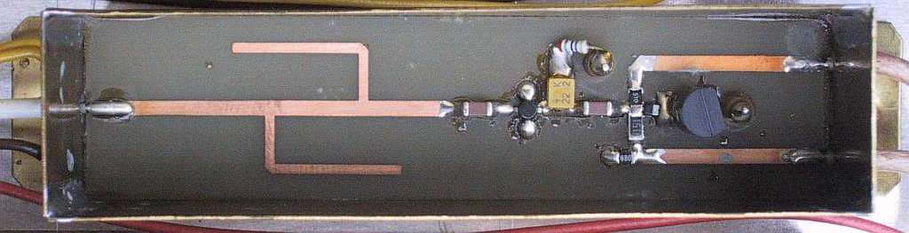
Except for the PLL logic, all other modules use microstrip circuit boards. Some of the latter were already described in the spectrum-analyzer article, while the new ones are shown on Fig.8. All microstrip boards are etched on one side of a 0.8mm thick FR4 glassfiber-epoxy laminate, while the other side is not etched to act as a groundplane. The PLL logic is built on a single-sided board shown on Fig.9 and etched on 0.8mm thick FR4 laminate.
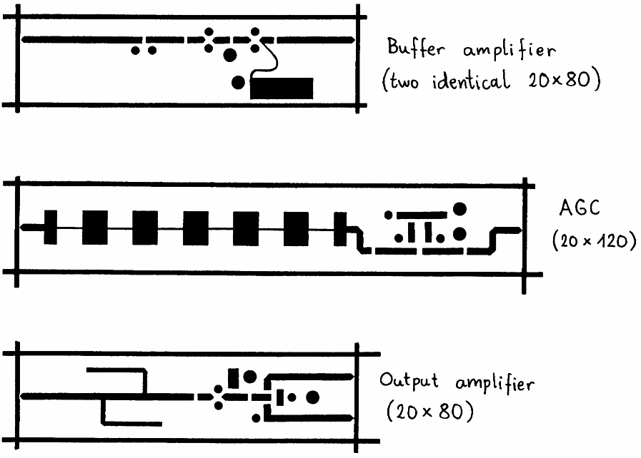
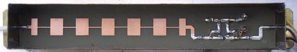
Fig.8 - Microstrip circuit boards (150dpi).
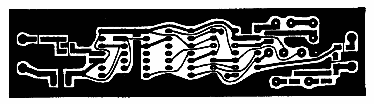
Fig.9 - PLL logic PCB (30X120, 150dpi).
Microwave absorber foam is built under the cover of two modules: buffer amplifier for the wide-band (2.1...3.85GHz) VCO and output mixer. Other modules usually do not require any absorber foam inside. Microwave absorber is also not required in the space among the shielded boxes.
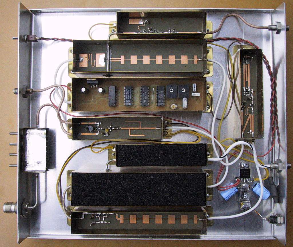
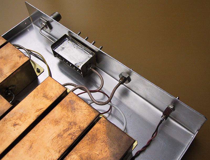
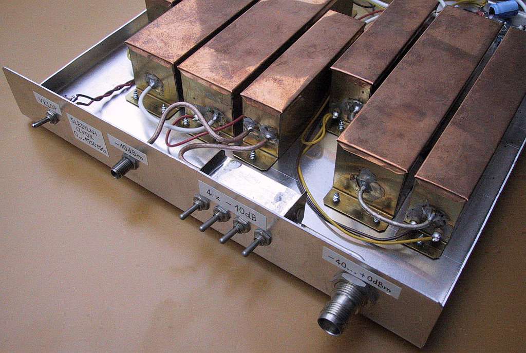
The tracking-generator module location is shown on Fig.10. The tracking generator has the same depth (240mm) and width (220mm) as the spectrum analyzer, so that the two boxes can be stacked easily one over another. The height of the tracking generator is only 32mm, since all modules are located in a single plane. The bottom of the box is simply a piece of 1mm thick aluminum sheet, bent in the form of an "U". The cover is a similar "U" made from 0.6mm thick aluminum sheet.
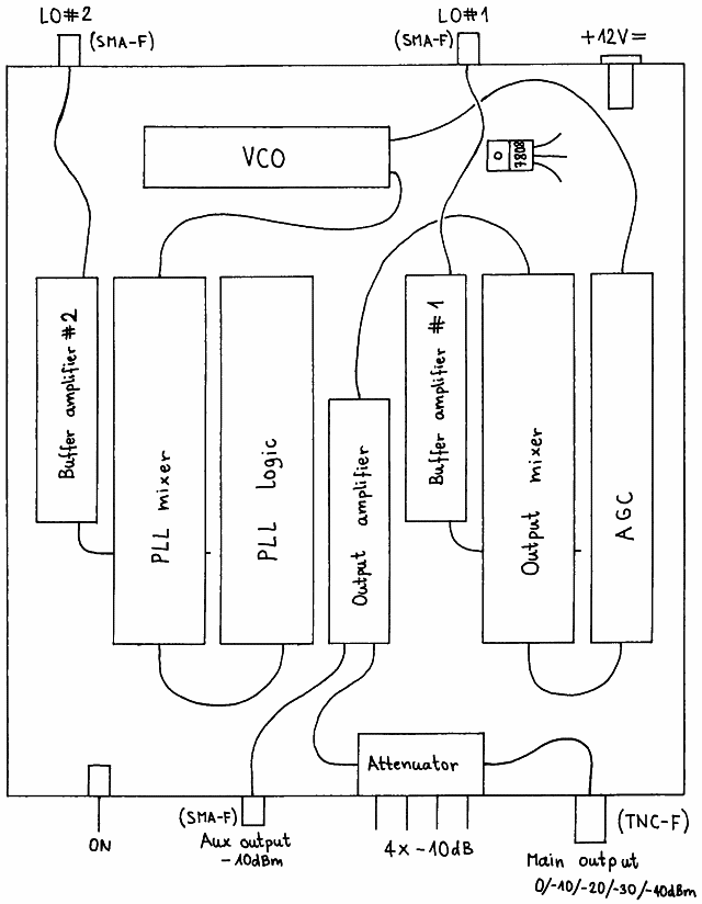
Fig.10 - Tracking-generator module location.
6. Alignment and checkout
The tracking generator is a much simpler piece of test equipment than the spectrum analyzer. Correspondingly the alignment and checkout should be much simpler too. Of course, the spectrum analyzer should be available at all times to supply the signals of both VCOs. Before connecting all tracking-generator modules together, it makes sense to make a few simple checks on each module separately.
In all modules it makes sense to check the DC bias points of all semiconductors. Most simple errors can be detected in this way. Next some RF checks can be performed. Both buffer amplifiers should be checked for the output RF power level when driven by the corresponding VCO in the spectrum analyzer.
The VCO needs a fine tuning of the frequency coverage, since the microstrip board was originally designed for a slightly lower frequency in the spectrum analyzer. Of course, the operating frequency of the VCO should be monitored while carefully shortening the base and collector strips. The VCO should achieve the nominal operating frequency of 2.1GHz at a tuning voltage of 3...3.5V. Further, the VCO should operate without dropouts through the whole range of tuning voltages 0...+5V. Some trimming of the center finger (with the BB833 varactor) may also be required.
In the PLL logic, the operation of the crystal oscillator should be checked first. Both 1kohm trimmers should be set initially with the sliders on the respective "hot" ends, to allow the widest span of the output voltage Vf. Without any input signal Vf should reach almost +5V. If a frequency above 70.7MHz is fed to the input (for example a grid-dip meter coupled through a small wire loop), the Vf output should drop to zero.
Using the already tested modules, the 2.1GHz PLL can be assembled and tested. While the PLL is locked, the DC voltage on the LOCK test point should drop to less than 0.2V. Both 1kohm trimmers in the PLL logic are then set for a frequency coverage of +/-60MHz around the nominal frequency of 2100MHz. While testing the PLL, the main output of the VCO should be terminated properly on a matched load.
After the alignment of the PLL is completed, the remaining modules of the tracking generator can be wired together. The latter do not include any alignment points, but their operation should be verified. The spectrum analyzer should be set to scan the whole frequency band 0...1750MHz with the widest (4MHz) IF filter. While connecting the output of the tracking generator to the input of the spectrum analyzer, the whole trace should raise almost to the full scale. The trace will not be perfectly straight. The required fine adjustments to flatten the response will be described later.
The next step is to test the tracking generator with narrower IF filters. There will probably be no change with a 700kHz IF bandwidth. However, the response will probably drop with narrower IF filters. The response should be brought back to its original value by adjusting the crystal oscillator in the PLL logic. If the range of the trimmer is insufficient, a parallel capacitor may be added or the trimmer may be replaced with an adjustable inductor. In the worst case, the crystal in the PLL logic and/or the 60MHz crystal in the spectrum analyzer may have to be replaced.
In order to check the operation of the AGC, the Y input of the oscilloscope (used as the display of the spectrum analyzer) is temporarily connected to the AGC line. Although the AGC voltage may span 0...+8V, it should remain in the range +1...+3V in a correctly-operating tracking generator. A too high or too low AGC voltage may suggest what is actually wrong with the tracking generator. While testing the AGC voltage, the main output of the tracking generator should be terminated to a matched load. If the main output is left unterminated, the AGC voltage may move out of the required +1...+3V range.
The main checkout of the tracking generator is completed at this point. However, several minor adjustments may be necessary both in the tracking generator and in the spectrum analyzer to optimize the operation. In particular, the frequency response of the spectrum analyzer should be flattened as much as possible. Without any adjustments, the response of the tracking generator connected directly to the spectrum analyzer may deviate by as much as +/-5dB.
Amplitude variations of the frequency response of the spectrum analyzer are mainly caused by the first mixer and its termination impedances. Additional impedance matching may flatten the overall response and/or move dips to compensate upward bumps in the response. Some dips and bumps move quickly while changing the length of the cable connecting the first mixer to the cavity filter. Small pieces of copper foil, soldered to the output microstrip of the wide-band VCO module, are usually very efficient in improving the impedance matching of the LO mixer port.
A substantial mismatch, especially above 1GHz, is also caused by the two step attenuators with toggle switches. Above 1GHz it is therefore recommended to use the aux -10dBm output to avoid at least one of the two step attenuators. A better solution is to connect external, fixed 10dB microwave attenuators (with SMA connectors) to both the tracking-generator output and the spectrum-analyzer input.
After all described fine adjustments, the frequency response of the tracking generator and spectrum analyzer connected together should be within +/-2dB from 100kHz to 1.6GHz. The decay above 1.6GHz is caused by the low-pass on the input of the spectrum analyzer. An accuracy of +/-2dB is reasonable even for much more expensive professional spectrum analyzers.
Of course, since the response of the spectrum analyzer and tracking generator can be measured easily, the resulting error can simply be subtracted from the real measurement result. Most manufacturers therefore offer an electronic storage/normalizer unit to be connected between the spectrum analyzer and the oscilloscope display. An electronic storage/normalizer (using cheap integrated circuits) was also developed and built for the described spectrum analyzer and tracking generator.
Original full-size drawings

References:
[1] Matjaz Vidmar: "Spectrum analyser 0...1750MHz", pages 2-30/1-99, VHF-Communications.
[2] Matjaz Vidmar: "Spektrum-Analyzer von 0 bis 1750MHz, Teil 1: Aufbau der Baugruppen", pages 18-30/4-99, AMSAT-DL Journal.
[3] Matjaz Vidmar: "Spektrum-Analyzer von 0 bis 1750MHz, Teil 2: Anzeigebaugruppen und Abgleich", pages 18-29/1-00, AMSAT-DL Journal.
* * * * *